Metallized polycrystalline silicon infrared micro-bolometer and preparation method thereof

A technology of microbolometer and polysilicon, applied in the direction of final product manufacturing, sustainable manufacturing/processing, climate sustainability, etc. Technical complexity and other issues, to achieve the effect of improving infrared absorption rate, low power consumption, and enhancing infrared absorption efficiency

Active Publication Date: 2021-07-16
NANJING UNIV
View PDF5 Cites 0 Cited by
  • Summary
  • Abstract
  • Description
  • Claims
  • Application Information

AI Technical Summary

Problems solved by technology

Traditional microbolometers based on MEMS technology have problems such as incompatibility between sensors and readout circuits, high processing costs, and complicated process technology, which largely hinder their wide application in related fields.
Infrared detectors prepared based on silicon integrated circuit technology can realize high-performance and highly integrated microbolometers, but silicon technology is limited by materials. For example, although the existing heat-sensitive material amorphous silicon is compatible with integrated circuit technology, it cannot It has high electronic noise. In addition, metal aluminum can also be used as another thermal material compatible with integrated circuits, but it has ultra-low resistivity. The characteristics of these materials lead to the performance of the prepared silicon-based infrared thermal sensor far lower than that of non- Prepared by standard process

Method used


Image

  • Metallized polycrystalline silicon infrared micro-bolometer and preparation method thereof
  • Metallized polycrystalline silicon infrared micro-bolometer and preparation method thereof
  • Metallized polycrystalline silicon infrared micro-bolometer and preparation method thereof

Examples


Embodiment Construction

[0024] In order to make the object, technical solution and advantages of the present invention clearer, the implementation manner of the present invention will be further described in detail below in conjunction with the accompanying drawings. Apparently, the described embodiments are only some of the embodiments of the present invention, not all of them. The described embodiments are for illustration only and do not limit the scope of the invention. Based on the embodiments of the present invention, all other embodiments obtained by persons of ordinary skill in the art without making creative efforts belong to the protection scope of the present invention.

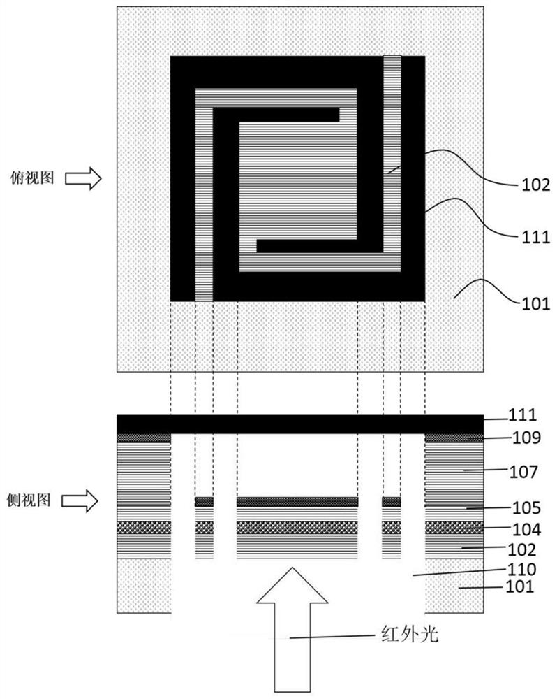
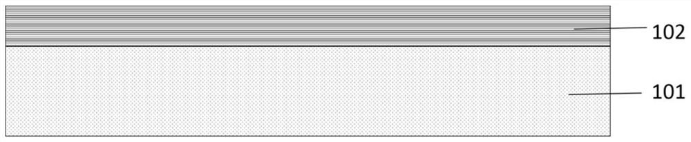
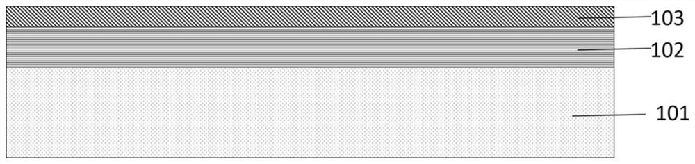
[0025] Such as figure 1 As shown, the metallized polysilicon infrared microbolometer structure of the present invention includes metallized polysilicon 104 , silicon dioxide 102 , 105 , silicon nitride 109 and metal aluminum 111 . The entire structure is designed on single crystal silicon 101 compatible with standard in...


PUM

PropertyMeasurementUnit
thicknessaaaaaaaaaa
thicknessaaaaaaaaaa
thicknessaaaaaaaaaa

Abstract

The invention discloses a metalized polycrystalline silicon infrared micro-bolometer and a preparation method thereof. The micro-bolometer comprises a silicon substrate, an absorbing body and a reflecting layer, wherein the absorbing body is located above the silicon substrate, and is of a stacked structure composed of silicon dioxide/metalized polycrystalline silicon/silicon dioxide/silicon nitride, the reflecting layer is arranged above the absorbing body, and a cavity is formed between the reflecting layer and the absorbing body. The absorption-enhanced metalized polycrystalline silicon infrared micro-bolometer can be prepared by a standard integrated circuit process technology, can realize high integration of functions, is low in power consumption, and has a cost advantage.

Description

technical field [0001] The invention relates to an infrared microbolometer structure, in particular to a metallized polysilicon infrared microbolometer structure and a preparation method thereof based on an integrated circuit technology for enhanced absorption. Background technique [0002] Infrared microbolometer has the characteristics of room temperature operation, wide response band, and excellent performance. It has a wide range of application values ​​in military, meteorology, earth environment, agriculture, medicine and other fields. The infrared microbolometer consists of two parts: an infrared absorber and a resistance sensor. When the infrared light is irradiated on the surface of the absorber, the temperature of the absorber rises, resulting in a change in the temperature of the resistance, and this change realizes infrared detection through signal reading. [0003] Whether the microbolometer uses a single pixel or an array chip, a readout circuit based on a sili...

Claims


Application Information

Patent Timeline
Patent Type & Authority Applications(China)
IPC IPC(8): H01L31/101H01L31/18H01L31/0216
CPCH01L31/101H01L31/1804H01L31/02161Y02P70/50
Inventor 纪小丽罗明成闫锋石东海
Owner NANJING UNIV
Why Eureka
Try Eureka