

Active edge grip rest pad
- Summary
- Abstract
- Description
- Claims
- Application Information
AI Technical Summary
Benefits of technology
Problems solved by technology
Method used
Image

Examples
Embodiment Construction
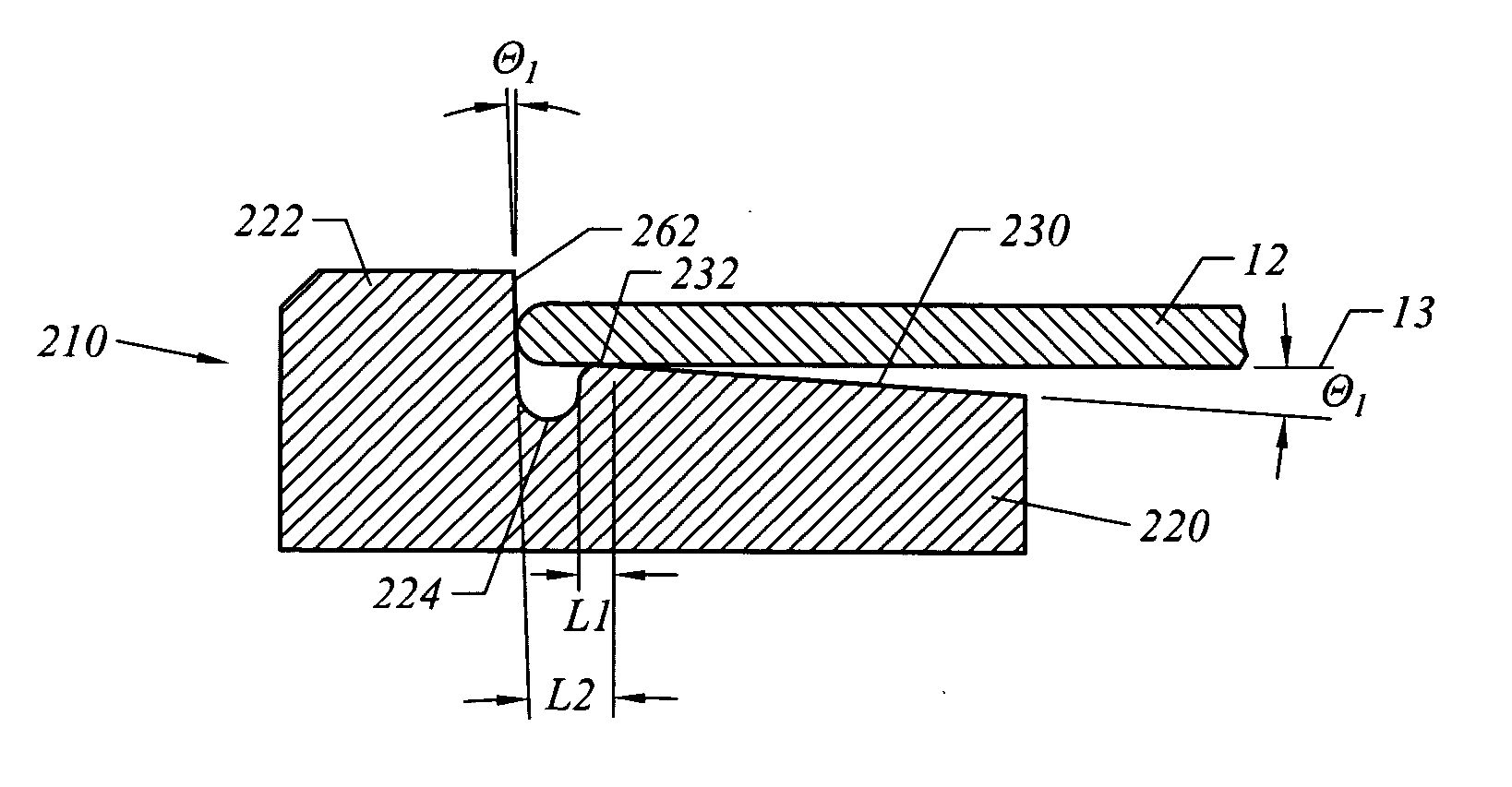
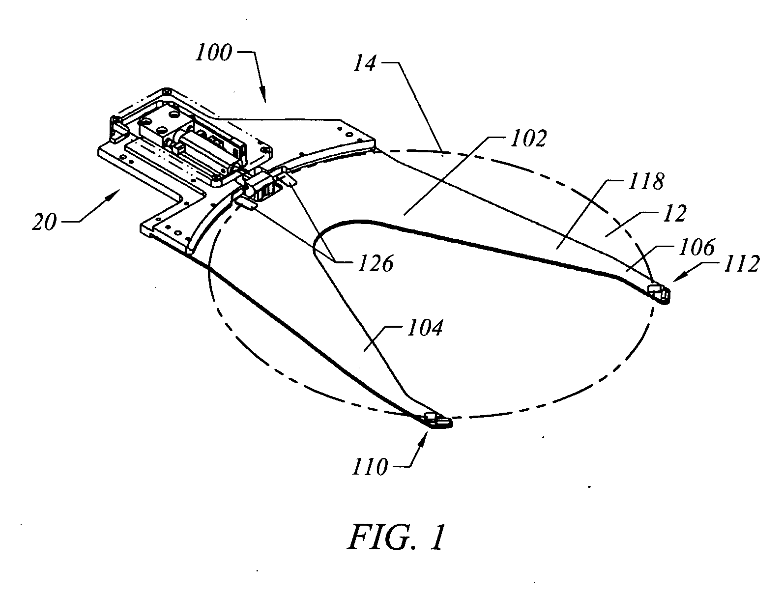
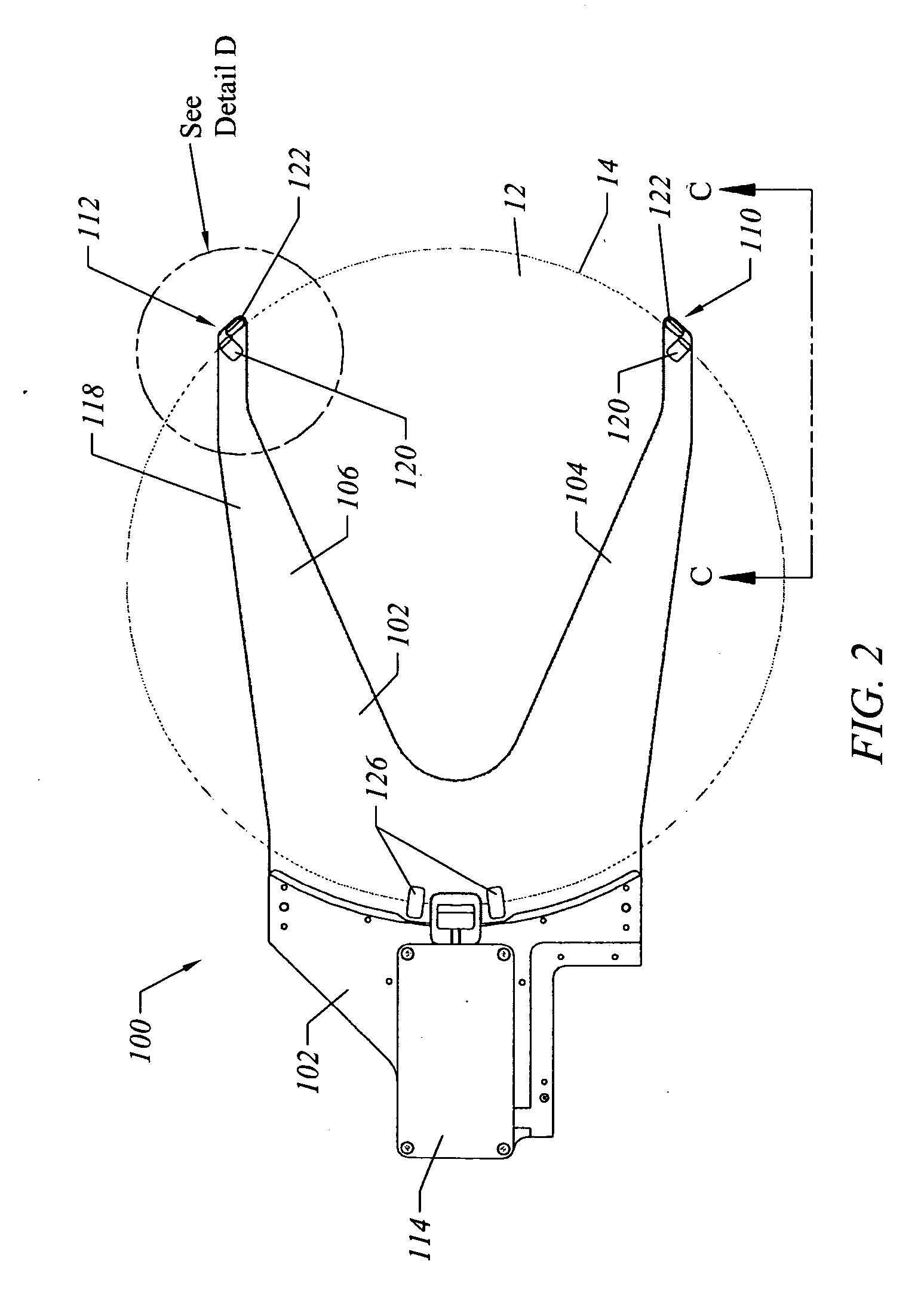
[0029]FIGS. 1-2 illustrate an embodiment of an end effector. The end effector 100 generally comprises a support plate 102 having a first finger 104 and a second finger 106 located at a distal end 110 of the support plate 102. Mounting holes are located throughout the support plate 102. As will be discussed in more detail later, each mounting hole is adapted to receive a specific element (e.g., distal rest pad, proximal rest pad, etc.). The end effector 100 shown in FIGS. 1-2 is merely an example and the present invention is not limited for use with this specific configuration.
[0030] The end effector 100 is configured to support and transport a wafer 12. In order to support a wafer 12, the end effector 100 includes, among other things, a first distal rest pad 110 and a second distal rest pad 112, a pair of proximal rest pads 126, and a pusher device 114. The pusher device 114 urges a wafer 12 seated on the support plate 102 towards the first distal rest pad 110 and the second distal...
PUM
 Abstract
Description
Claims
Application Information