

Method of forming contact hole and method of fabricating semiconductor device
a technology of contact hole and semiconductor device, which is applied in the field of forming contact hole and fabricating semiconductor device, to achieve the effect of avoiding short circuit problems of devices
- Summary
- Abstract
- Description
- Claims
- Application Information
AI Technical Summary
Benefits of technology
Problems solved by technology
Method used
Image

Examples
Embodiment Construction
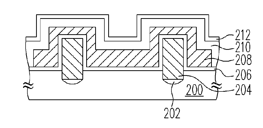
[0021]FIGS. 2A-2E are schematic cross sectional views showing progress of a method of fabricating a semiconductor device according to an embodiment of the present invention.
[0022] Referring to FIG. 2A, plural source regions 202 are formed in the substrate 200, and plural device structures 204 are formed over the source regions 202. Wherein, the method of forming the source regions 202 can be an ion implantation method, for example. In addition, the device structures 204 can be trench-type structures partially formed in the substrate 200, or the device structures (not shown) formed over the surface of the substrate 200. Further, the device structures 204 can be gate structures or conductive line structures. Wherein, the gate structure includes, for example, at least one dielectric layer and a gate layer; and the conductive line structure includes, for example, at least one conductive layer. A dielectric layer 206 and a conductive layer 208 are then sequentially formed over the devic...
PUM
 Abstract
Description
Claims
Application Information