
Method for manufacturing a semiconductor device

a manufacturing method and semiconductor technology, applied in the direction of semiconductor devices, electrical apparatus, transistors, etc., can solve the problems of trench processing accuracy, inferior alicyclic structure to aromatic ring etching resistance, and inability to find any route for electric charge accumulated in the body to escape, etc., to improve the processing accuracy of the first, simplify the process, and facilitate the alignment between the third window and the fourth opening.

Inactive Publication Date: 2006-03-07
FUJITSU SEMICON LTD
View PDF7 Cites 4 Cited by
  • Summary
  • Abstract
  • Description
  • Claims
  • Application Information

AI Technical Summary

Benefits of technology

"The present invention provides a method for manufacturing a semiconductor device by using a second mask layer with high etching selectivity to improve the stability of a first photoresist pattern. The second mask layer is constituted by a silicon layer that can be etched at lower ion energy than other layers, reducing damage to the photoresist. The method includes forming a first mask layer on a semiconductor layer, a silicon layer as a second mask layer, and a first photoresist pattern. The second mask layer is then etched through the first photoresist pattern, resulting in a second opening in the second mask layer. A second trench is formed in self-align manner to the second opening, improving processing accuracy. The second trench is also formed with high accuracy even when using a light with longer wavelength than ArF. The method simplifies the process by eliminating the need for additional removal of the second mask layer. Additionally, a thicker polysilicon layer prevents pinholes from being formed and improves processing accuracy. A silicon dioxide layer absorbs stresses from a silicon nitride layer, preventing cracking of the semiconductor layer."

Problems solved by technology

However, if the SOI MOS transistor is completely isolated by the device isolation insulating layer and the buried insulating layer as described above, the silicon layer (body) in the region which is surrounded by these insulating layers and is served as the transistor forming region is electrically floating, and the electric charge accumulated in the body cannot find any route to escape.
Therefore, the above-described alicyclic structure is employed in ArF photoresist, but an alicyclic structure is inferior to an aromatic ring in etching resistance.
Accordingly, despite the use of ArF exposure suitable for miniaturization, the processing accuracies of the trenches 201a are deteriorated and, ultimately, devices cannot be miniaturized.

Method used


Image

  • Method for manufacturing a semiconductor device
  • Method for manufacturing a semiconductor device
  • Method for manufacturing a semiconductor device

Examples


first embodiment

(1) First Embodiment

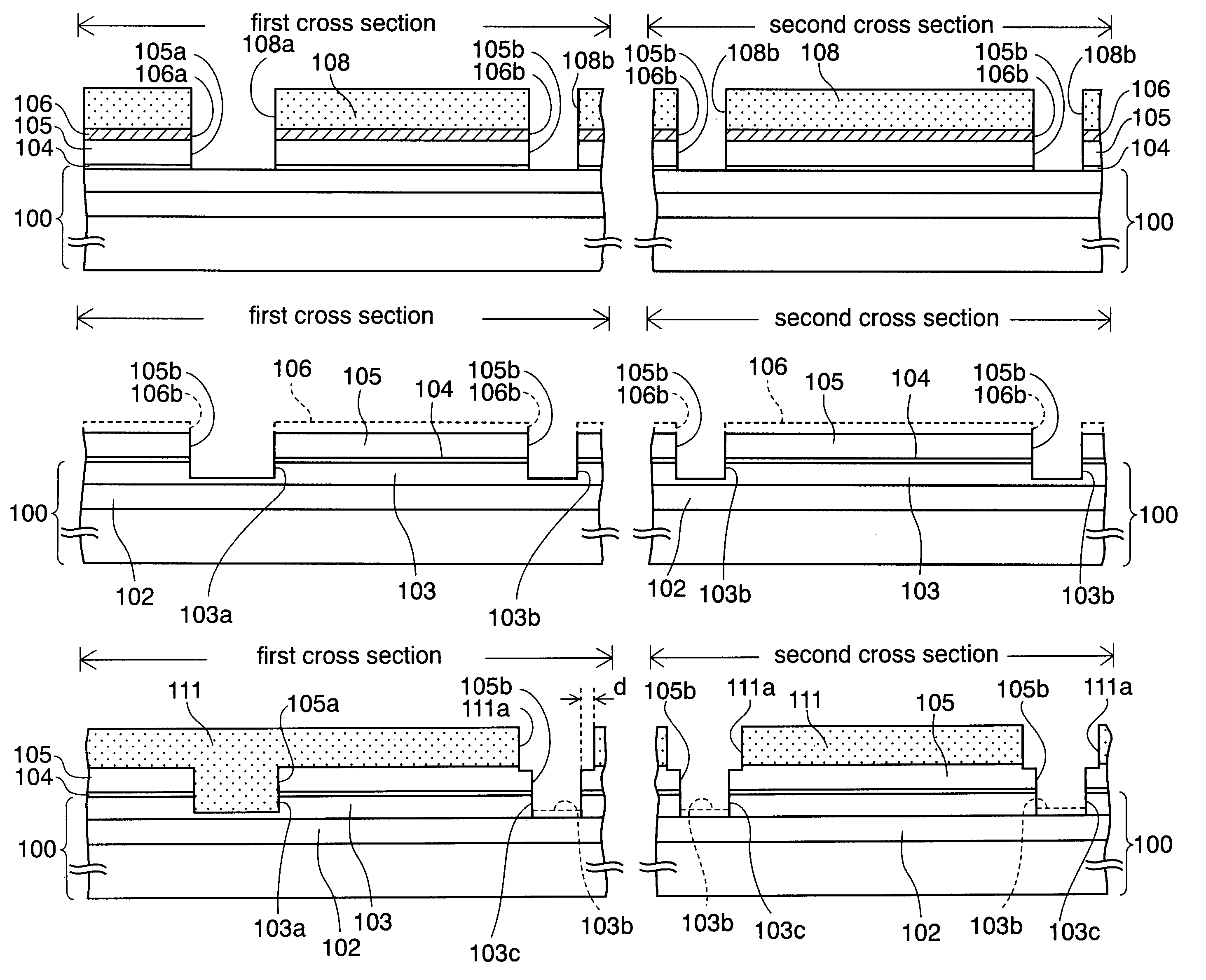
[0043]FIGS. 3A to 3T are cross-sectional views showing steps in a manufacturing method of a semiconductor device according to an embodiment of the present invention. In each of these drawings, for convenience of explanation, both of a first cross section taken along the gate width direction of a MOS transistor and a second cross section taken along the gate length thereof are shown. Moreover, the semiconductor device has a structure in which n-channel MOS transistors and p-channel MOS transistors coexist, but only the cross section of an n-channel MOS transistor is illustrated below. Furthermore, FIGS. 4 to 7, which are plan views corresponding to respective steps, are also referred to as needed.

[0044]To begin with, steps before the cross-sectional structure shown in FIG. 3A is obtained will be described.

[0045]First, a silicon substrate (not shown) having a thermally-oxidized film, which is to be a buried insulating layer 102, with a thickness of approximately 10...

second embodiment

(2) Second Embodiment

[0139]In the first embodiment already described, the partial trench 103a and the full trench 103c is formed as two types of trenches having different depths in the SOI substrate 100. However, the present invention is not limited to this. As described below, two types of trenches having different depths may be formed in a silicon substrate by applying the method of the first embodiment to the silicon substrate instead of the SOI substrate. Hereinafter, advantages obtained in this case will be described.

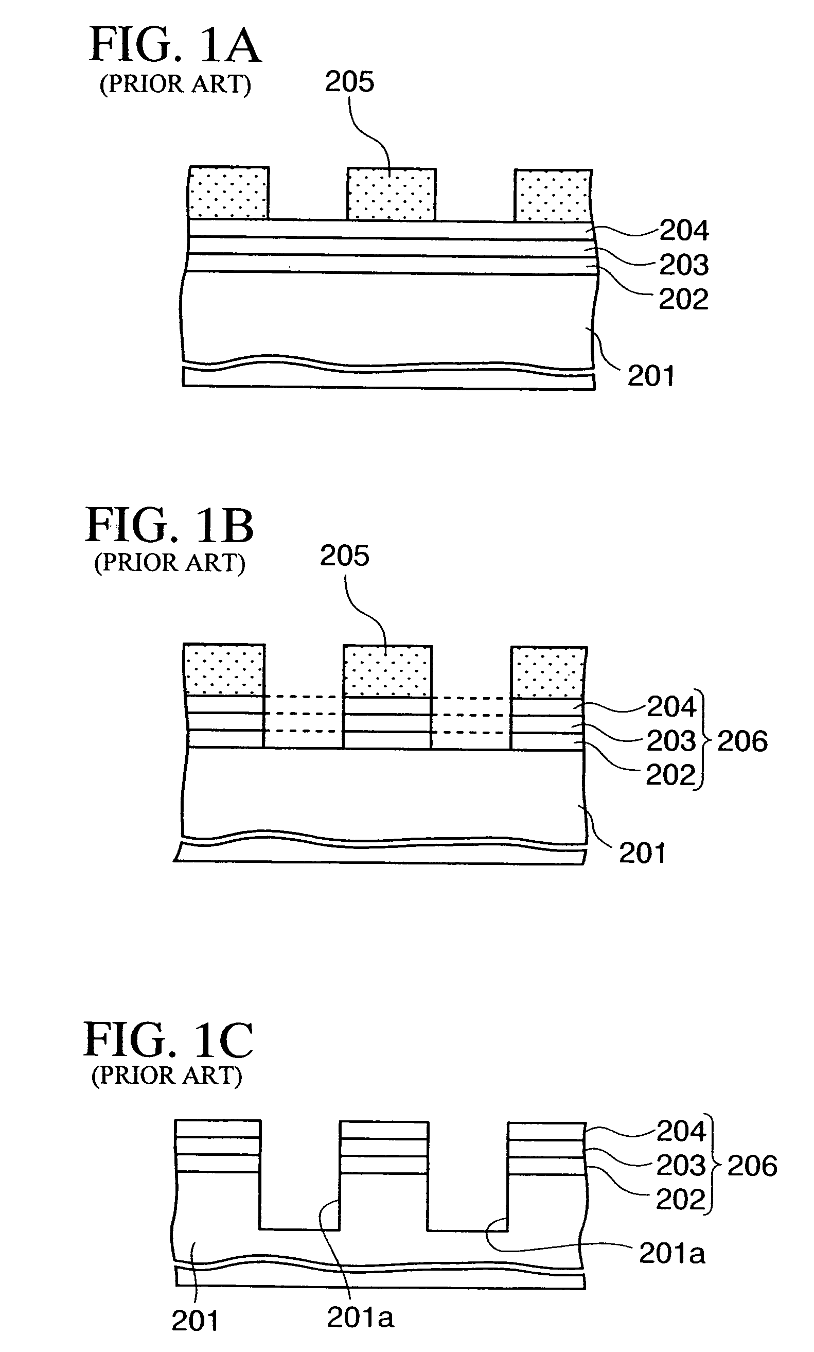
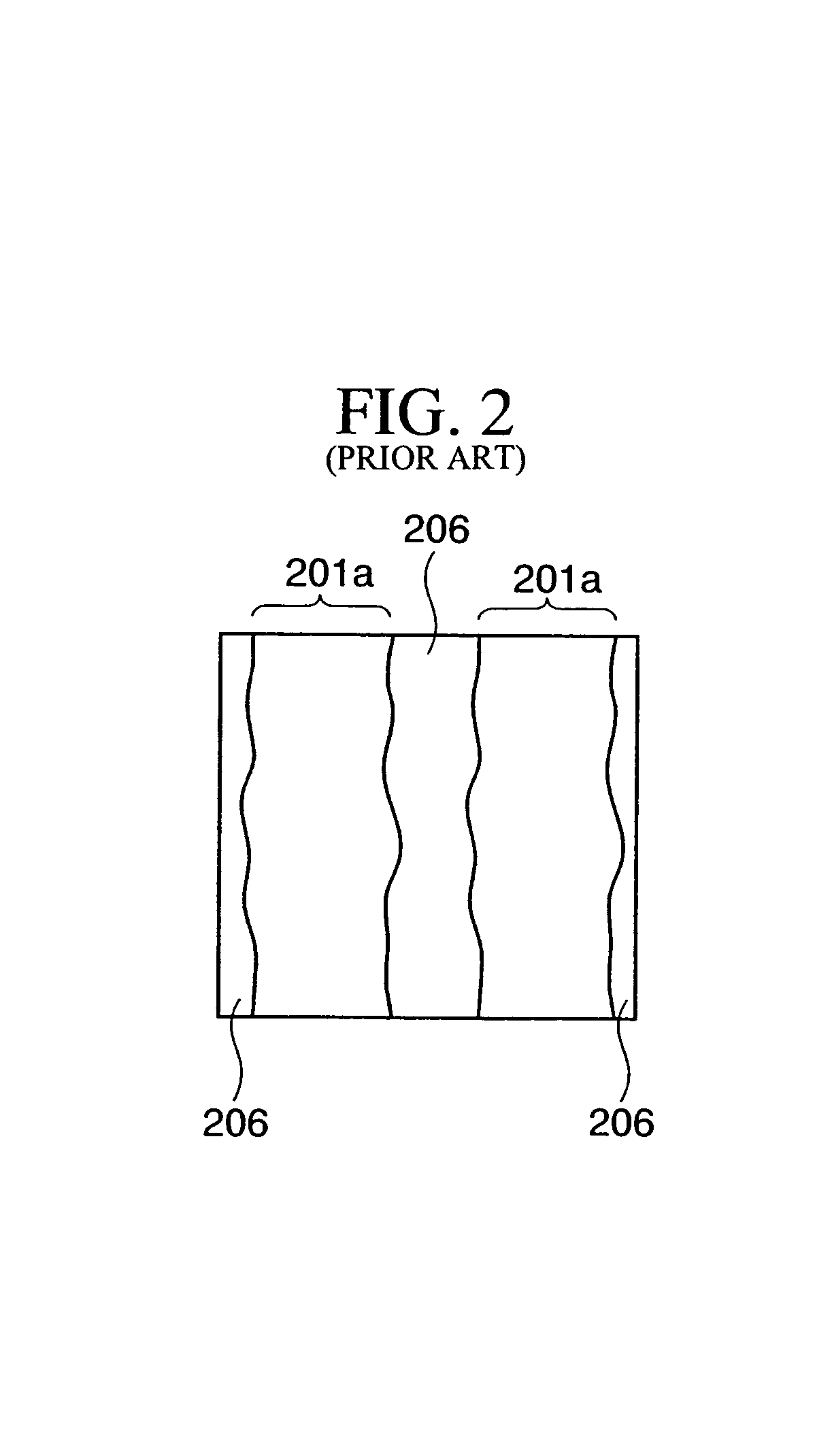
[0140]FIG. 11 is a cross-sectional view in the case where p-channel MOS transistors and n-channel MOS transistors are formed on a silicon substrate 130 through a general CMOS process without adopting the first embodiment.

[0141]In order to obtain this cross-sectional structure, to begin with, first and second trenches 130a and 130b for shallow trench isolation (STI) are simultaneously formed to the same depth in the p-type silicon substrate 130. After that, the tren...


PUM


Abstract

A method for manufacturing a semiconductor device includes: forming a first photoresist pattern on a second hard mask by use of ArF; forming first and second openings in the second hard mask by use of the first photoresist pattern as an etching mask; forming third and fourth openings in a first hard mask under the first and second openings; forming a partial trench (first trench) and a trench for a full trench (second trench) in an SOI substrate (semiconductor substrate) under the first and second openings; and forming the trench for a full trench into a full trench by etching the trench for a full trench through the fourth opening exposed through a third window of a second photoresist pattern.

Description

CROSS-REFERENCE TO RELATED APPLICATIONS[0001]This application is based on and claims priority of Japanese Patent Application No. 2003-386006 filed on Nov. 14, 2003, the entire contents of which are incorporated herein by reference.BACKGROUND OF THE INVENTION[0002]1. Field of the Invention[0003]The present invention relates to a method for manufacturing a semiconductor device. More specifically, the present invention relates to a method for manufacturing a semiconductor device in which two types of trenches having different depths are formed in a semiconductor layer.[0004]2. Description of the Related Art[0005]Currently, semiconductor devices such as LSIs are typically fabricated by use of silicon substrates. However, in order to further improve device characteristics, the fabrication of LSIs using silicon-on-insulator (SOI) substrates is being actively researched.[0006]An SOI substrate has a structure in which a buried insulating layer and a silicon layer are formed in order on a su...

Claims


Application Information

Patent Timeline
Patent Type & Authority Patents(United States)
IPC IPC(8): H01L21/00H01L21/76H01L21/336H01L21/762H01L21/84H01L27/08H01L27/12H01L29/786
CPCH01L21/76283H01L21/84H01L29/78654H01L29/66772H01L29/78609H01L27/1203
Inventor NAKAI, SATOSHISAKUMA, JUNTAJIMA, MITSUGU
Owner FUJITSU SEMICON LTD
Learn More