Using electrically programmable fuses to hide architecture, prevent reverse engineering, and make a device inoperable

a technology of electrically programmable fuse and architecture, applied in the direction of unauthorized memory use protection, instruments, error detection/correction, etc., can solve the problems of unauthorized methods, less complex chips can be problematic, and manufacture a single chip for multiple complex applications, so as to prevent copying of proprietary information and prevent unauthorized access

Active Publication Date: 2006-06-22
MARVELL ASIA PTE LTD
View PDF1 Cites 54 Cited by
  • Summary
  • Abstract
  • Description
  • Claims
  • Application Information

AI Technical Summary

Benefits of technology

[0011] The present invention generally relates methods and systems that allow operation of and/or access to particular features of an electronic device to be controlled after the device has left the control of a device manufacturer.
[0012] One embodiment provides a method for preventing unauthorized access to selected internal components of an integrated circuit device. The method generally includes blowing at least one electrically programmable fuse in the integrated circuit device, wherein the electrically programmable fuse is configured to control externally generated communication between a communication interface of the integrated circuit device and the selected internal components of the integrated circuit device.
[0013] Another embodiment provides a method for preventing copying of proprietary information from an integrated circuit device. The method generally includes determining if a first unauthorized access attempt to secure information on the integrated circuit device has occurred, setting a first tamper bit if the first unauthorized access attempt is determined, modifying a first device parameter in accordance with the first tamper bit, determining if a second unautho

Problems solved by technology

However, these test interfaces often provide an interface or “backdoor” for a hardware hacker, i.e., a person unauthorized to access information contained in the device, to gain access to the device, and more particularly, to gain access to the manufacturer's proprietary information embedded in the device.
However, from a business standpoint, manufacturing a single chip for multiple complex applications and disabling the more advanced portions of complex chips used in configurations of lesser complexity can be problematic, as chip hackers may exploit the use of the more advanced chip in a configuration of less complexity, e.g., the hackers will use unauthorized methods to unlock the disabled modules of the chip.
Further, in some cases, hacking may resul

Method used


Image

  • Using electrically programmable fuses to hide architecture, prevent reverse engineering, and make a device inoperable
  • Using electrically programmable fuses to hide architecture, prevent reverse engineering, and make a device inoperable
  • Using electrically programmable fuses to hide architecture, prevent reverse engineering, and make a device inoperable

Examples


Embodiment Construction

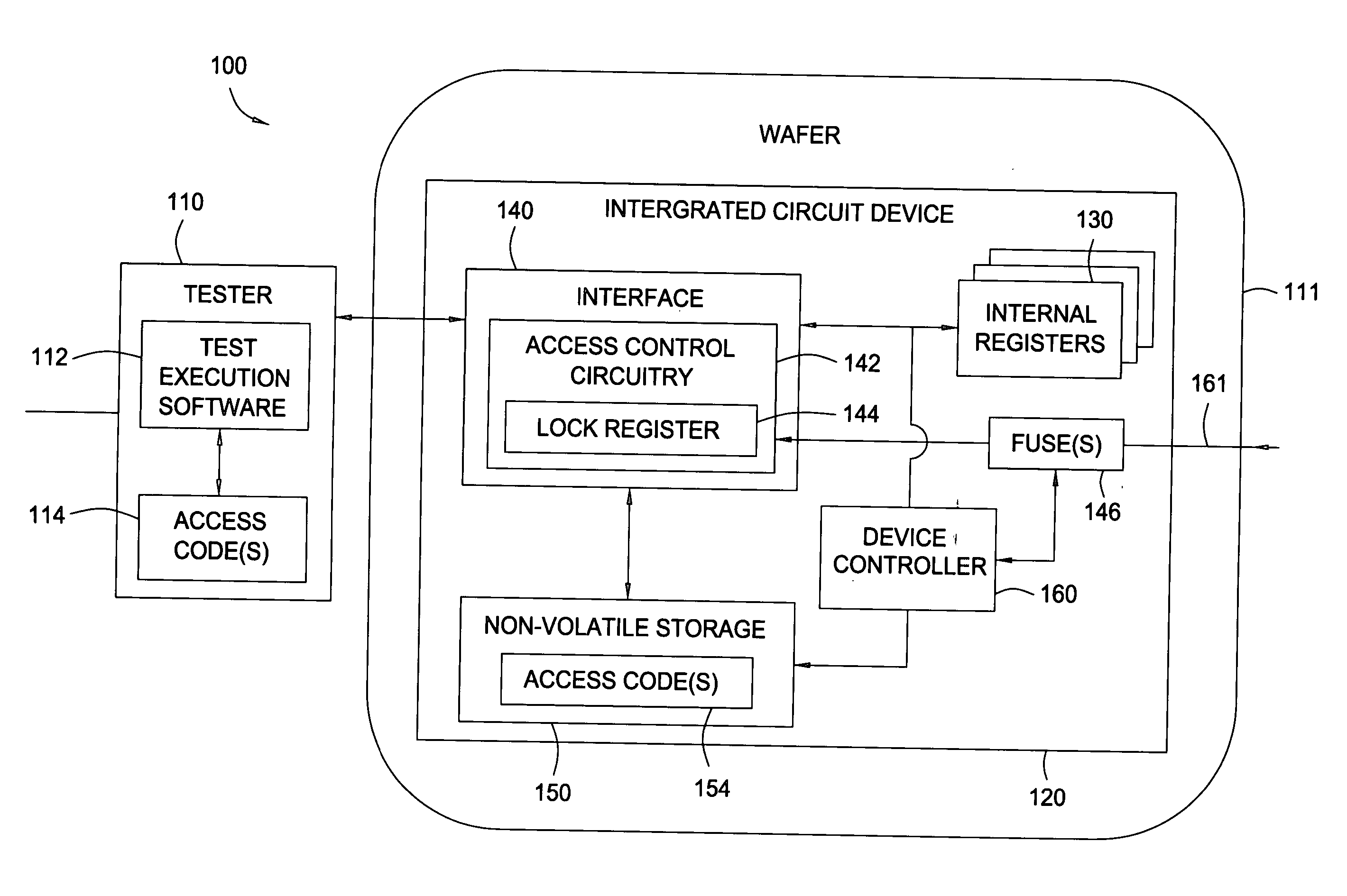
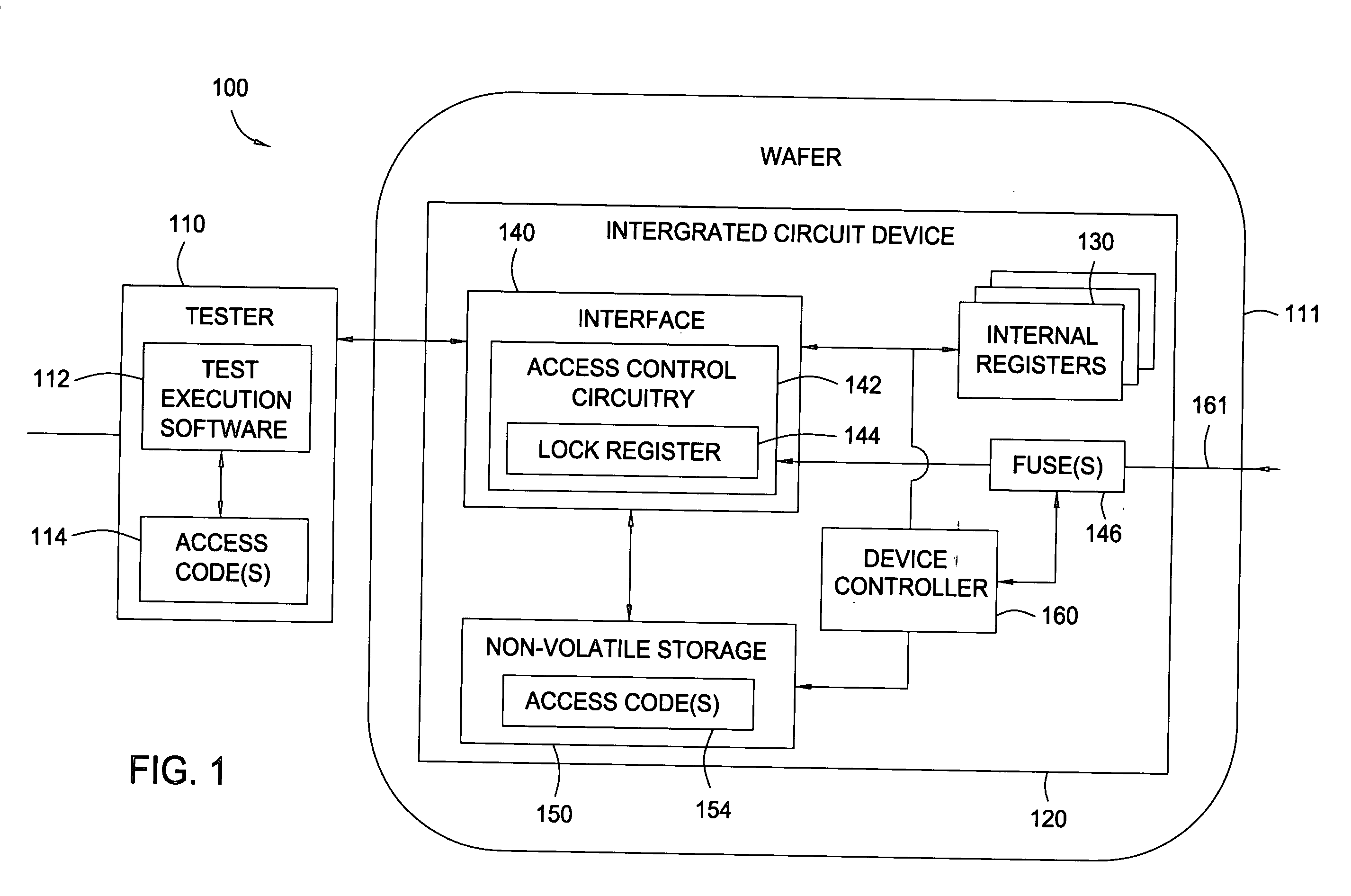
[0024] Embodiments of the present invention provide techniques and systems whereby operation of and / or access to particular features of an electronic device may be controlled after the device has left the control of the manufacturer. The device may include a set of non-volatile storage elements, such as electronically programmable fuses (hereinafter eFUSES) that may be programmed to control the operation of or access to these features. According to some embodiments, a purposeful set of reconfiguration may be initiated by the manufacturer in order to enable chip functionality and / or minimize data bottlenecks in order to reduce test cost. For some embodiments, power and performance device characteristics for each device may be determined during manufacturing testing and each device may be subsequently configured accordingly for specific applications.

[0025] In the following, reference is made to embodiments of the invention. However, it should be understood that the invention is not l...


PUM


Abstract

Techniques and systems whereby operation of and/or access to particular features of an electronic device may be controlled after the device has left the control of the manufacturer are provided. The operation and/or access may be provided based on values stored in non-volatile storage elements, such as electrically programmable fused (eFUSES).

Description

CROSS-REFERENCE TO RELATED APPLICATIONS [0001] This application is related to commonly owned U.S. patent applications entitled “Changing Chip Function Based on Fuse States” (Atty Docket No. ROC920040272US1) and “Utilizing Fuses to Store Control Parameters for External System Components” (Atty Docket No. ROC920040332US1), both filed herewith and incorporated herewith by reference.BACKGROUND OF THE INVENTION [0002] 1. Field of the Invention [0003] The present invention generally relates to integrated circuit devices, and more particularly, to methods and systems for preventing unauthorized access to proprietary information contained in the integrated circuit devices after the devices have left the manufacturing facility. [0004] 2. Description of the Related Art [0005] Many integrated circuit (IC) devices, such as systems on a chip (SOC) and other types of very large scale integration (VLSI) and ultra large scale integration (ULSI) devices include interfaces that allow for access to th...

Claims


Application Information

Patent Timeline
IPC IPC(8): G06F12/14G06F21/75G06F21/86
CPCG06F12/1433G06F21/6245
Inventor BONACCIO, ANTHONY R.ERICKSON, KARL R.FIFIELD, JOHN A.KOTHANDARAMAN, CHANDRASEKHARANPAONE, PHIL C.TONTI, WILLIAM R.
Owner MARVELL ASIA PTE LTD
Why Eureka
Try Eureka