
Lithographic apparatus and device manufacturing method

a technology of lithographic apparatus and manufacturing method, which is applied in the direction of instruments, radiation therapy, therapy, etc., can solve the problems of difficult thermal control, inefficiency of beam splitters, and inability to use different polarizations to create different effects

Inactive Publication Date: 2006-06-29
ASML NETHERLANDS BV +1
View PDF13 Cites 42 Cited by
  • Summary
  • Abstract
  • Description
  • Claims
  • Application Information

AI Technical Summary

Benefits of technology

The present invention provides a lithographic apparatus that uses an array of individually controllable elements to pattern a radiation beam. The apparatus includes an illumination system, an array of elements, and a projection system. The illumination system conditions a beam of radiation, the array of elements patterns the beam, and the projection system projects the patterned beam onto a target portion of a substrate. The radiation beam can be non-perpendicularly illuminated onto the array of elements, and can change the telecentricity or optical axis of the beam. The apparatus can be used in a method for manufacturing devices by patterning a beam of radiation and projecting it onto a substrate. The technical effects of this invention include improved precision and accuracy in patterning a radiation beam, and improved efficiency in manufacturing devices.

Problems solved by technology

Use of the polarization to control the direction of the radiation beam means that the cross section of the radiation beam has a uniform polarization, and thus different polarizations cannot be used to create different effects during the exposure.
Also, beam splitters are inefficient and can be difficult to thermally control.
A non-polarizing beam splitter, with a half silvered mirror, can be used instead of a polarizing beam splitter to avoid polarization issues, but with two passes through such a device about 75% or more of the radiation is lost, substantially reducing throughput.

Method used


Image

  • Lithographic apparatus and device manufacturing method
  • Lithographic apparatus and device manufacturing method
  • Lithographic apparatus and device manufacturing method

Examples


Embodiment Construction

Overview and Terminology

[0028] Throughout the remainder of this specification the terms “alignment mark” and “alignment marks” will be used to denote one or more individual, indiscrete alignment marks respectively, unless otherwise stated. By “individual” it is meant that each alignment mark is separate and distinct from others of its kind (i.e., from the other alignment marks). By “indiscrete” it is meant that each alignment mark is not divided into parts (e.g., each alignment mark is a single, undivided entity). A variety of such marks can be used in embodiments of the invention, and it will be appreciated that the dots, dashes, and lines referred to in this specification are merely specific examples. Other forms can be used.

[0029] Although specific reference can be made in this text to the use of lithographic apparatus in the manufacture of integrated circuits (ICs), it should be understood that the lithographic apparatus described herein can have other applications, such as t...


PUM

PropertyMeasurementUnit
angleaaaaaaaaaa
wavelengthaaaaaaaaaa

Abstract

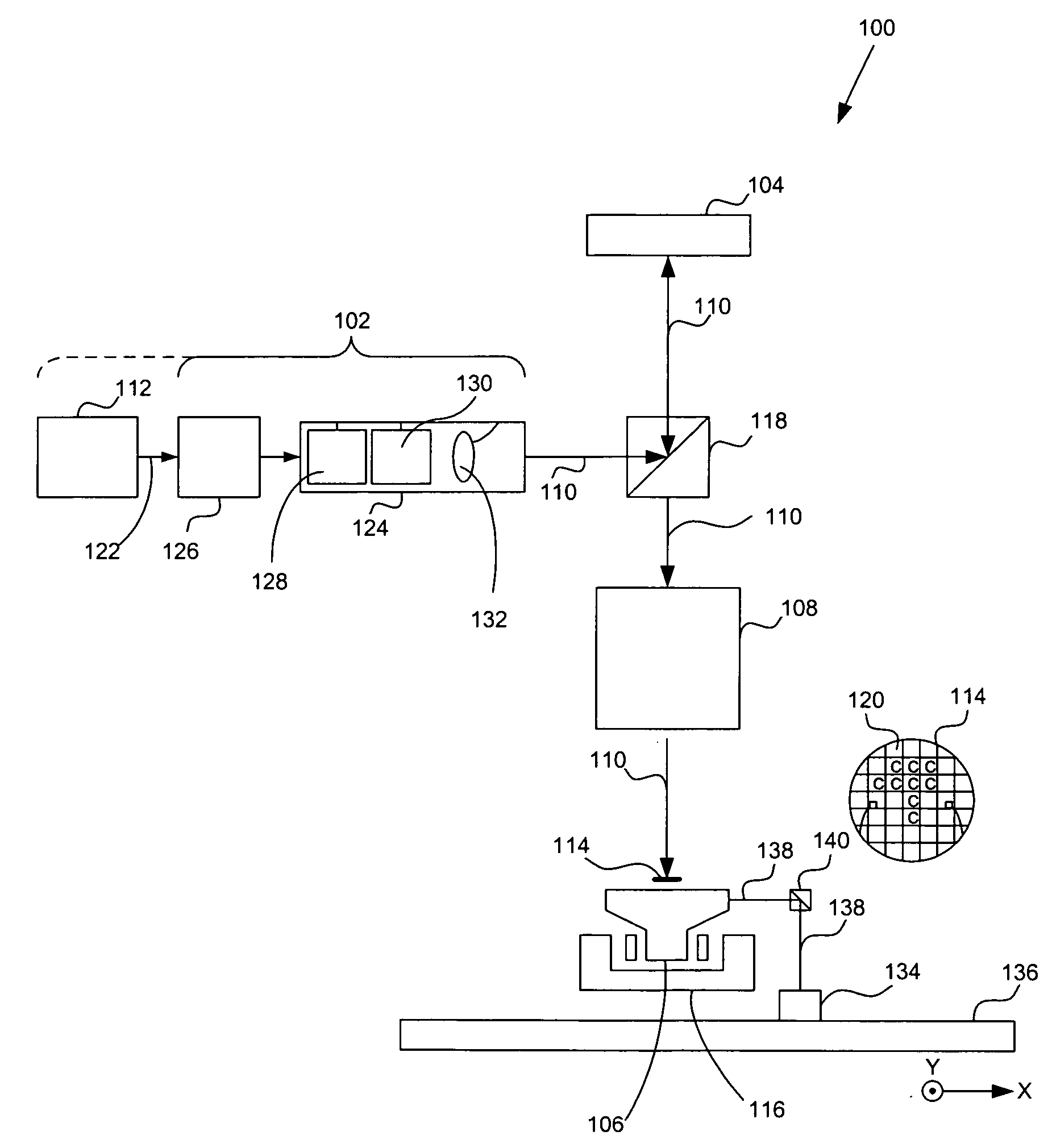
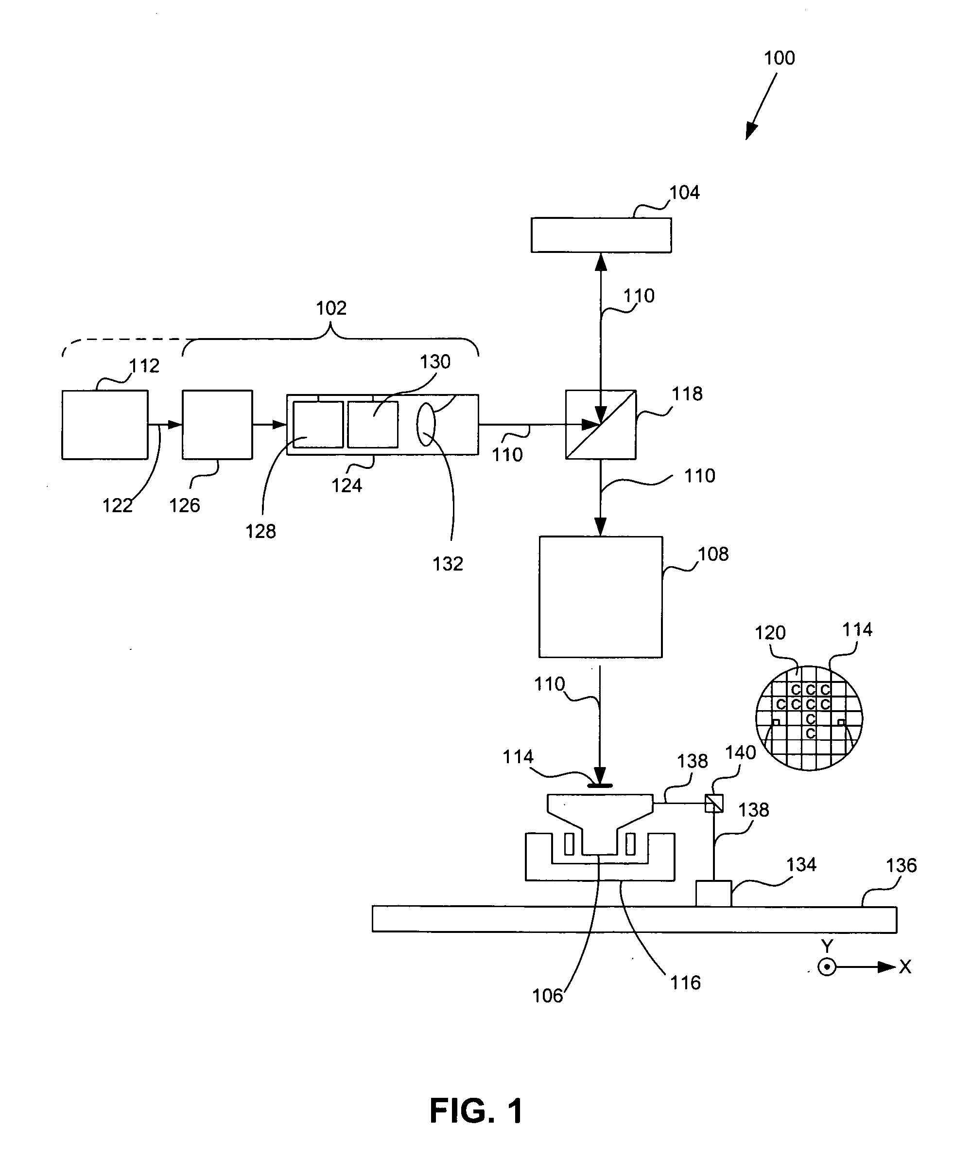
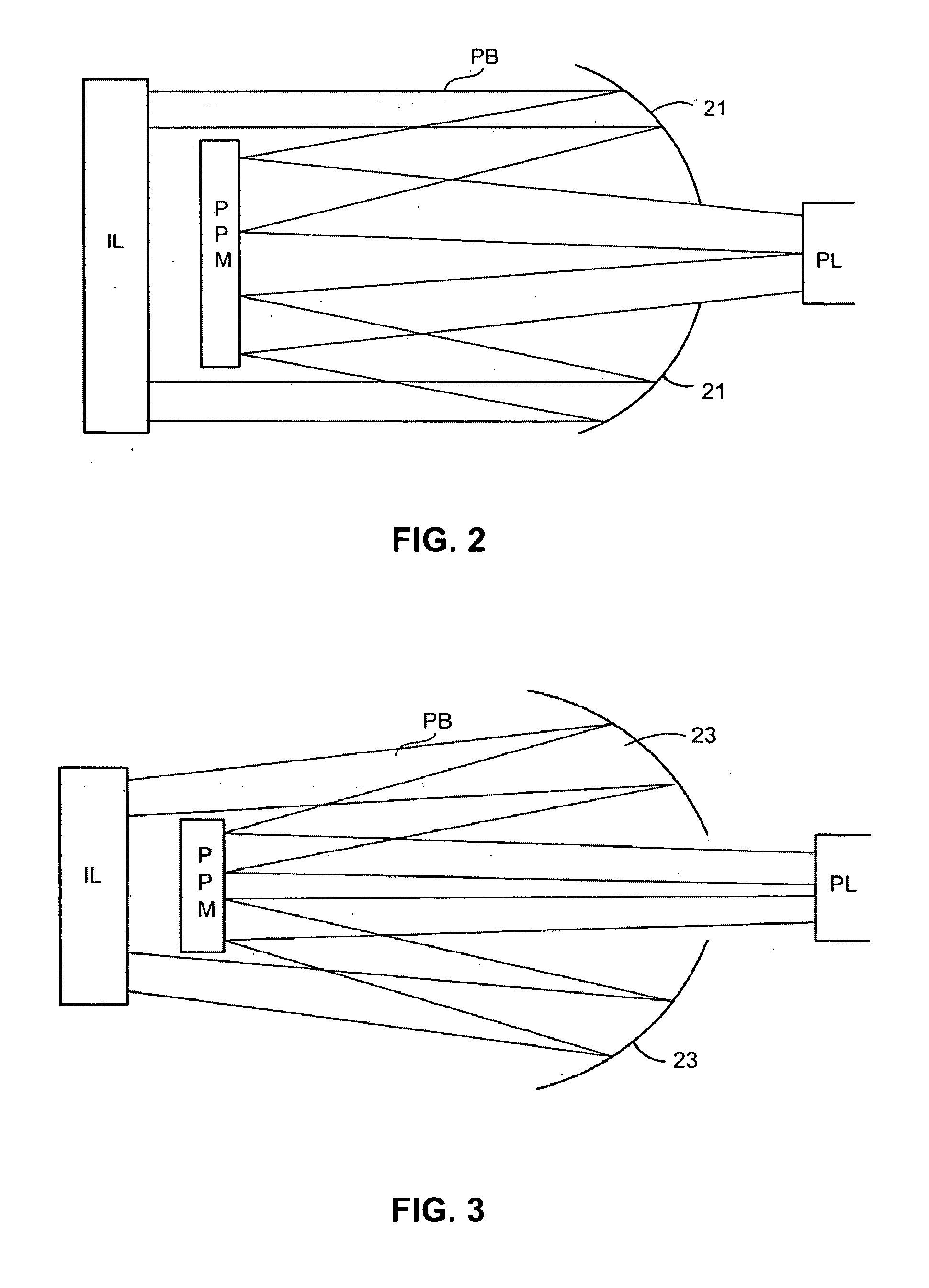
A system and method are used to direct a radiation beam to illuminate non-perpendicularly a patterning array of individually controllable elements used for patterning the radiation beam. The individually controllable elements can change a telecentricity of the radiation beam. Projection of the radiation beam onto the individually controllable elements can be by a concave mirror or use a folding mirror placed in an object field of the individually controllable elements. Alternatively, the individually controllable elements can change the optical axis of the radiation beam.

Description

BACKGROUND [0001] 1. Field of the Invention [0002] The present invention relates to a lithographic apparatus and a device manufacturing method. [0003] 2. Related Art [0004] A lithographic apparatus is a machine that applies a desired pattern onto a target portion of a substrate. The lithographic apparatus can be used, for example, in the manufacture of integrated circuits (ICs), flat panel displays, and other devices involving fine structures. In a conventional lithographic apparatus, a patterning means, which is alternatively referred to as a mask or a reticle, can be used to generate a circuit pattern corresponding to an individual layer of the IC (or other device), and this pattern can be imaged onto a target portion (e.g., comprising part of one or several dies) on a substrate (e.g., a silicon wafer or glass plate) that has a layer of radiation-sensitive material (e.g., resist). Instead of a mask, the patterning means can comprise an array of individually controllable elements t...

Claims


Application Information

Patent Timeline
Patent Type & Authority Applications(United States)
IPC IPC(8): G03F7/20
CPCG03F7/702G03F7/70291
Inventor BLEEKER, ARNO JANBASELMANS, JOHANNES JACOBUS MATHEUSDIERICHS, MARCE MATHIJS THEODORE MARIESMIRNOV, STANISLAVWAGNER, CHRISTIANRYZHIKOV, LEVTROOST, KARS ZEGER
Owner ASML NETHERLANDS BV
Learn More