Substrate processing apparatus and transfer positioning method thereof

a processing apparatus and positioning technology, applied in the direction of individual semiconductor device testing, semiconductor/solid-state device testing/measurement, instruments, etc., can solve the problems of insufficient height position accuracy and time-consuming steps, and achieve the effect of reducing steps involving visual observation and manual operation and improving height position accuracy

Active Publication Date: 2006-06-29
TOKYO ELECTRON LTD
View PDF2 Cites 2 Cited by
  • Summary
  • Abstract
  • Description
  • Claims
  • Application Information

AI Technical Summary

Benefits of technology

[0008] The present invention is made in view of the above-described problems, and is intended for providing a substrate processing apparatus and a transfer positioning method capable of reducing steps involving visual observation and manual operation by an operator during teaching as compared to conventional arts so as to perform teaching efficiently, as well as improving accuracy of height position.

Problems solved by technology

Since respective parts are modularized in the substrate processing apparatus as described above, positions, heights and so on of respective modules include some errors from design values when these modules are assembled.
However, also in this method, when performing the rough teaching or the like for example, there are steps involving visual observation and manual operation by an operator, and thus there is a problem requiring much time and labor in these steps.
Also, since the teaching using the orienter is for a horizontal direction, there is a problem such that accuracy of height (Z axis) position cannot be obtained adequately.

Method used


Image

  • Substrate processing apparatus and transfer positioning method thereof
  • Substrate processing apparatus and transfer positioning method thereof
  • Substrate processing apparatus and transfer positioning method thereof

Examples


Embodiment Construction

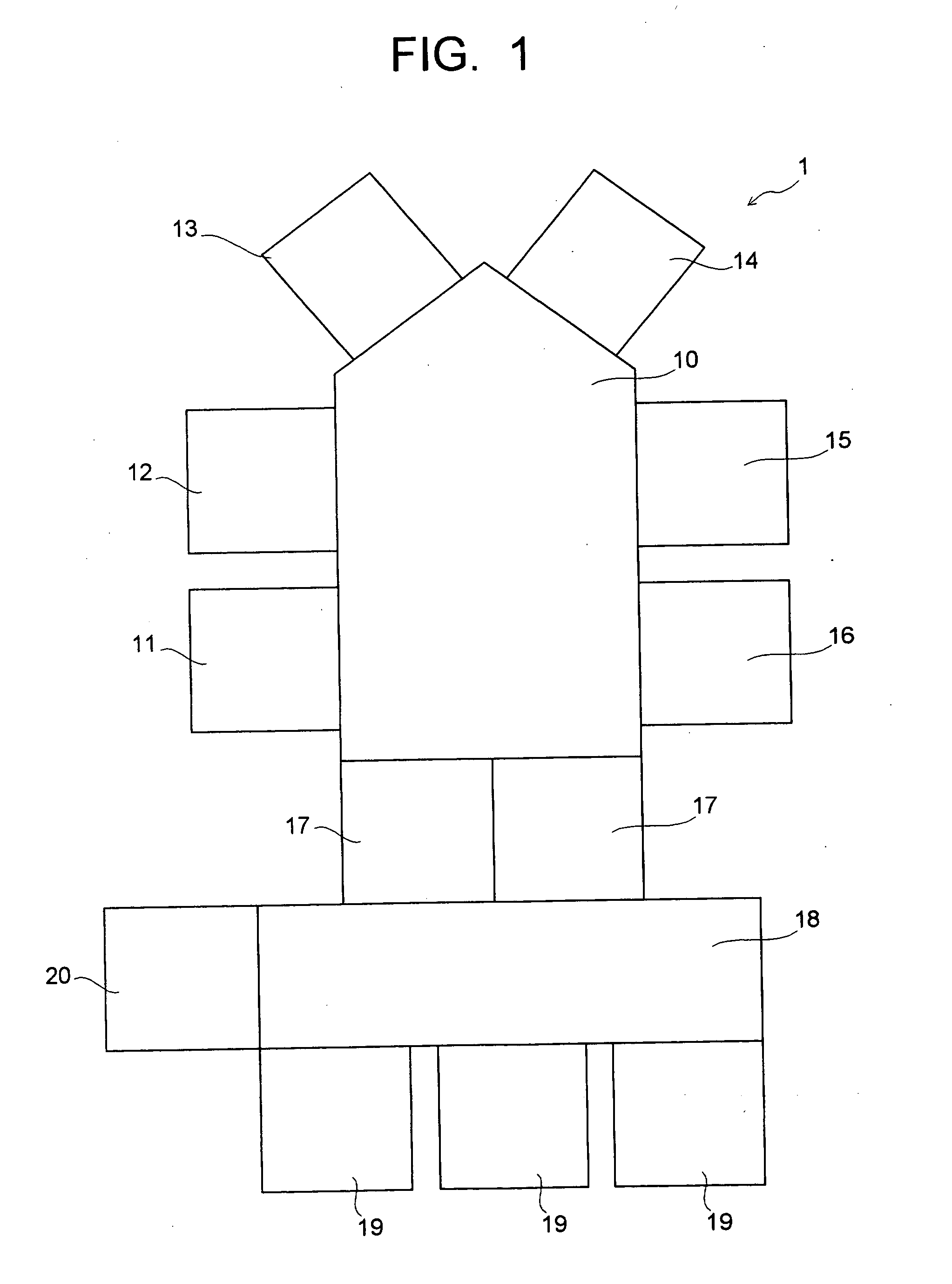
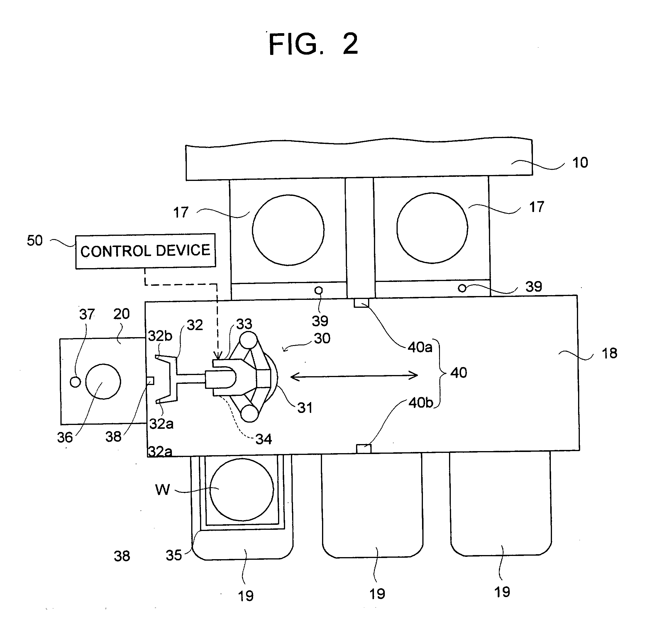
[0022] Hereinafter, details of the present invention with respect to one embodiment will be described with reference to the drawings. FIG. 1 is a view showing an overall structure of a substrate processing apparatus according to one embodiment of the present invention. As shown in FIG. 1, at a center part of a substrate processing apparatus 1, a vacuum transfer chamber 10 is provided, and along this vacuum transfer chamber 10, a plurality of (six in this embodiment) vacuum process chambers 11 to 16 are disposed in the vicinity thereof.

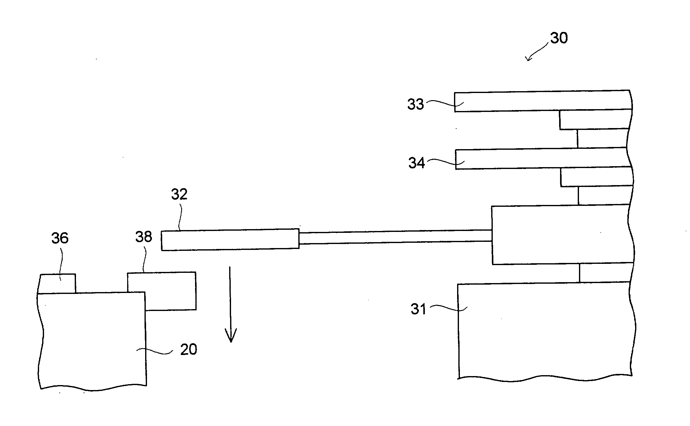
[0023] On a near side (lower side in the drawing) of the vacuum transfer chamber10, two load lock chambers 17 are provided. Further, on a nearer side (lower side in the drawing) of these load lock chambers 17, a transfer chamber 18 for transferring a semiconductor wafer W in the atmosphere is provided. Further, on a nearer side (lower side in the drawing) of this transfer chamber 18, a plurality of (three in FIG. 1) mounting parts 19 are provided, on ...


PUM

PropertyMeasurementUnit
heightaaaaaaaaaa
heightaaaaaaaaaa
heightsaaaaaaaaaa

Abstract

A substrate processing apparatus has a transfer mechanism arranged on a transfer base and configured to transfer a processing substrate between predetermined transfer positions, a mapping sensor arranged on the transfer base and configured to detect an arrangement state of a processing substrate inside a processing substrate accommodating case which accommodates a plurality of processing substrate in a shelf-like form, and a Z-axis teaching jig provided on or in the vicinity of one of the transfer positions. This substrate processing apparatus detects, by the mapping sensor, a height of the Z-axis teaching jig so as to perform teaching of Z-axis to the transfer mechanism with respect to the one of the transfer positions.

Description

CROSS-REFERENCE TO THE INVENTION [0001] This application is based upon and claims the benefit of priority from the prior Japanese Patent Application No. 2004-374955, filed on Dec. 24, 2004; and the prior U.S. Patent Provisional Application No. 60 / 662,777, filed on Mar. 18, 2005; the entire contents of which are incorporated herein by reference.BACKGROUND OF THE INVENTION [0002] 1. Field of the Invention [0003] The present invention relates to a substrate processing apparatus that performs processing such as etching, film-forming, or the like on a processing substrate such as a semiconductor wafer, a glass substrate for a liquid crystal display device or the like, and a transfer positioning method thereof. [0004] 2. Description of the Related Art [0005] Conventionally, substrate processing apparatuses are known, which perform processing such as etching, film-forming, or the like on a processing substrate that is a semiconductor wafer, a glass substrate for a liquid crystal display de...

Claims


Application Information

Patent Timeline
Patent Type & Authority Applications(United States)
IPC IPC(8): G01N21/86G01V8/00
CPCH01L21/67259
Inventor KONDOH, KEISUKE
Owner TOKYO ELECTRON LTD
Why Eureka
Try Eureka