
Light-emitting diode lamp and light-emitting diode display device

a technology of light-emitting diodes and display devices, which is applied in the direction of discharge tubes luminescnet screens, identification means, instruments, etc., can solve the problems of reducing the contrast ratio between lighting led lamps, degrading the display quality of led display boards that constitute electronic display boards, and becoming difficult to see led display boards. , to achieve the effect of improving visibility and improving luminous efficiency

Inactive Publication Date: 2006-06-29
SHARP KK
View PDF4 Cites 95 Cited by
  • Summary
  • Abstract
  • Description
  • Claims
  • Application Information

AI Technical Summary

Benefits of technology

[0012] An object of the present invention is to provide a diode lamp and a light-emitting diode display device capable of being utilized for display by increasing the luminous efficiency in the desired direction without any combination of complicated lens configurations.

Problems solved by technology

The phenomenon disadvantageously reduces the contrast ratio between the lighting LED lamp and the unlit LED lamp, and therefore it becomes sometimes difficult to see the LED display board.
The phenomenon resembles misrecognition of the traffic signal due to the west sun, and this significantly degrades the display quality of the LED display board that constitutes the electronic display board or the like.
However, this prior art example has consumed a lot of cost and time in production because complicated simulations and trial evaluations must be repeated for an appropriate lamp configuration every time the dimension of lamp is changed.
In the secondly-stated prior art example, the combination lens of the upper and lower portions having different curvatures repeatedly has required the complicated simulations and the trial evaluations for an appropriate configuration of lamp every time the dimension thereof is changed, which have consumed a lot of cost and time for developing new models.

Method used


Image

  • Light-emitting diode lamp and light-emitting diode display device
  • Light-emitting diode lamp and light-emitting diode display device
  • Light-emitting diode lamp and light-emitting diode display device

Examples


first embodiment

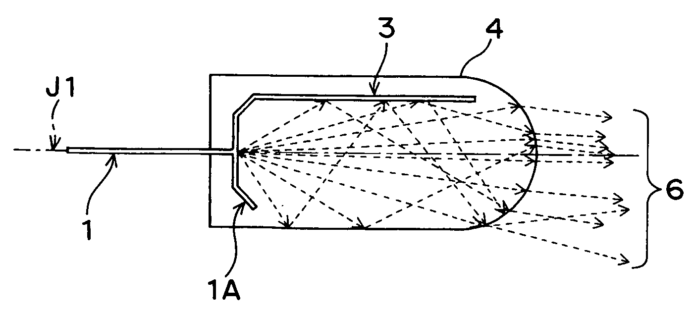
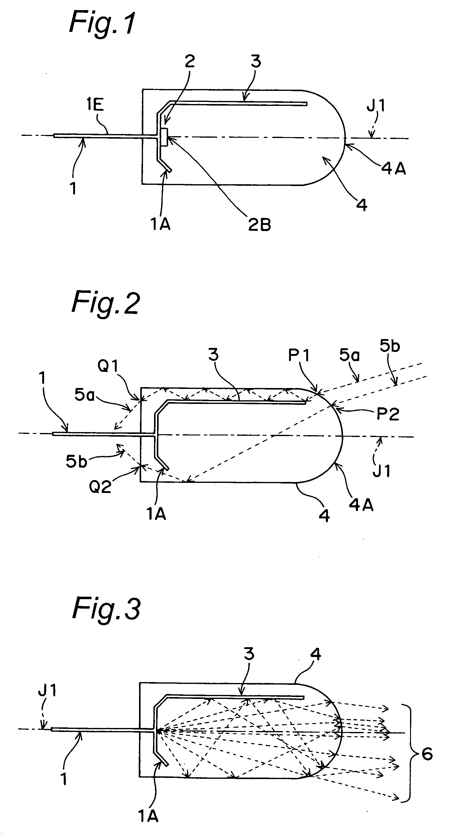
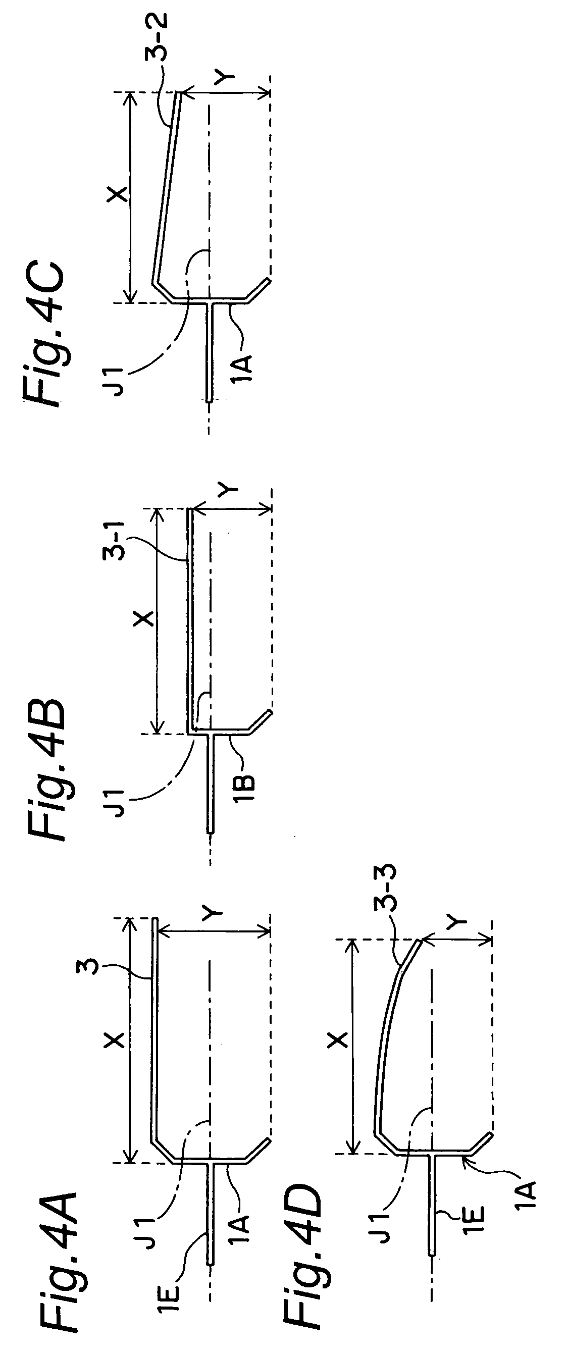
[0062]FIG. 1 shows a sectional view of the light-emitting diode lamp according to a first embodiment of the present invention viewed from a side. In the first embodiment, a light-emitting diode chip 2 is mounted on a cup-shaped mounting portion 1A of a lead frame 1. The mounting portion 1A is formed at one end in a direction in which a lead portion 1E of the lead frame 1 extends.

[0063] The light-emitting diode chip 2 and the mounting portion 1A are embedded in a resin-made convex lens 4 formed as a resin portion. Moreover, the lead frame 1 has a hood portion 3 served as a reflector. The hood portion 3 extends from the mounting portion 1A in a direction in which the lead portion 1E extends. The hood portion 3 is placed along an extension axis J1 in the direction in which the lead portion 1E extends and placed around the light-emitting diode chip 2. The hood portion 3 extends roughly parallel to the extension axis J1 above the extension axis J1 in FIG. 1. The hood portion 3 is not pl...

second embodiment

[0073]FIG. 5 shows a state in which a light-emitting diode lamp according to a second embodiment of the present invention is viewed from the front. FIG. 7 is a perspective view of the light-emitting diode lamp.

[0074] In the second embodiment, two light-emitting diode chips 21 and 22 are mounted on a mounting portion 11A of a lead frame 11. The two light-emitting diode chips 21 and 22 are connected to electrode leads 12 and 13 located on both sides of the lead frame 11 via connection wires 14 and 15, respectively.

[0075] As shown in FIG. 7, the mounting portion 11A and the two light-emitting diode chips 21 and 22 and the electrode leads 12 and 13 are embedded in the resin-made convex lens 17 as the resin portion. Moreover, the mounting portion 11A is formed at one end of a lead portion 11E of the lead frame 11.

[0076] The lead frame 11 has a hood portion 16 as a reflector. The hood portion 16 is placed along the extension axis J11 in the direction in which the lead portion 11E exten...

third embodiment

[0083]FIG. 6 shows a state in which the light-emitting diode lamp according to a third embodiment of the present invention is viewed from the front side.

[0084] In the third embodiment, the light-emitting diode lamp has a light-emitting diode chip 32 which is mounted on a mounting surface 31A of a mounting portion 31 of a lead frame 30. The light-emitting diode chip 32 is connected to the electrode lead 35 via a connection wire 34. The lead frame 30 has a lead portion (not shown). The lead portion extends depthwise in the normal line direction of the mounting surface 31A of the mounting portion 31 (i.e. in the rearward direction of the sheet of paper).

[0085] The mounting portion 31 of the lead frame 30, the light-emitting diode chip 32 and the electrode lead 35 are embedded in a resin-made convex lens 36 as a resin portion. The convex lens 36 has a convex configuration in the light-emitting direction of the light-emitting diode chip 32 (i.e. in the frontward direction of the sheet ...


PUM


Abstract

The light-emitting diode lamp has a light-emitting diode chip mounted on a cup-shaped mounting portion of a lead frame. The mounting portion is formed at one end of a lead portion of the lead frame. The light-emitting diode chip and the mounting portion are embedded in a convex shape lens made of a resin. The lead frame has a hood portion serving as a reflector. The hood portion downwardly reflects the outgoing beam of the light-emitting diode chip and also shields external incident light obliquely from the upper side. Thus, it is possible to increase the luminous efficiency in the downward direction, improve the visibility from the lower side and increase the luminous efficiency in the desired direction without any combination of complicated lens configurations.

Description

CROSS-REFERENCE TO RELATED APPLICATIONS [0001] This nonprovisional application claims priority under 35 U.S.C. §119(a) on Patent Application No. 2004-379260 filed in Japan on 28 Dec. 2004, the entire contents of which are incorporated herein by reference. BACKGROUND OF THE INVENTION [0002] The present invention relates to light-emitting diode lamps and light-emitting diode display devices, which are used for, for example, LED (light-emitting diode) display boards for outdoor purpose. They are suitably used for a road information display of traffic information and so on, an outdoor display for advertisement and publicity, or a traffic signal and so on. [0003] Conventionally, there has been an LED lamp as shown in FIG. 16. In the LED lamp, an LED chip 102 is mounted on a lead frame 101 and resin-molded to be embedded in a resin lens 103. The resin lens 103 has a curved surface 103A which is curved in a convex shape toward the light-emitting direction of the LED chip 102. [0004] When t...

Claims


Application Information

Patent Timeline
Patent Type & Authority Applications(United States)
IPC IPC(8): H01L33/00H01L33/56F21V5/04H01L33/58H01L33/60H01L33/62
CPCG09F9/33G09F2009/3055G09F2013/222H01L33/54H01L33/60H01L33/62H01L2224/48091H01L2924/3025H01L2924/00014H01L2924/12041H01L2224/48247
Inventor JYO, KATSUAKI
Owner SHARP KK
Features
  • Generate Ideas
  • Intellectual Property
  • Life Sciences
  • Materials
  • Tech Scout
  • Unparalleled Data Quality
  • Higher Quality Content
  • 60% Fewer Hallucinations
Learn More