Display device

Inactive Publication Date: 2006-06-29
TOSHIBA MATSUSHITA DISPLAY TECH
View PDF5 Cites 43 Cited by
  • Summary
  • Abstract
  • Description
  • Claims
  • Application Information

AI Technical Summary

Benefits of technology

[0008] The present invention has been made in consideration of the above-described problem, and the object of the invention is to provide a display device that can achieve a dec

Problems solved by technology

However, there are restrictions to the decrease in line widths and inter-line gaps, in consideration of the precision in patterning and the manufacturing yield.
It is thus very diffi

Method used


Image

  • Display device
  • Display device
  • Display device

Examples


embodiment 1

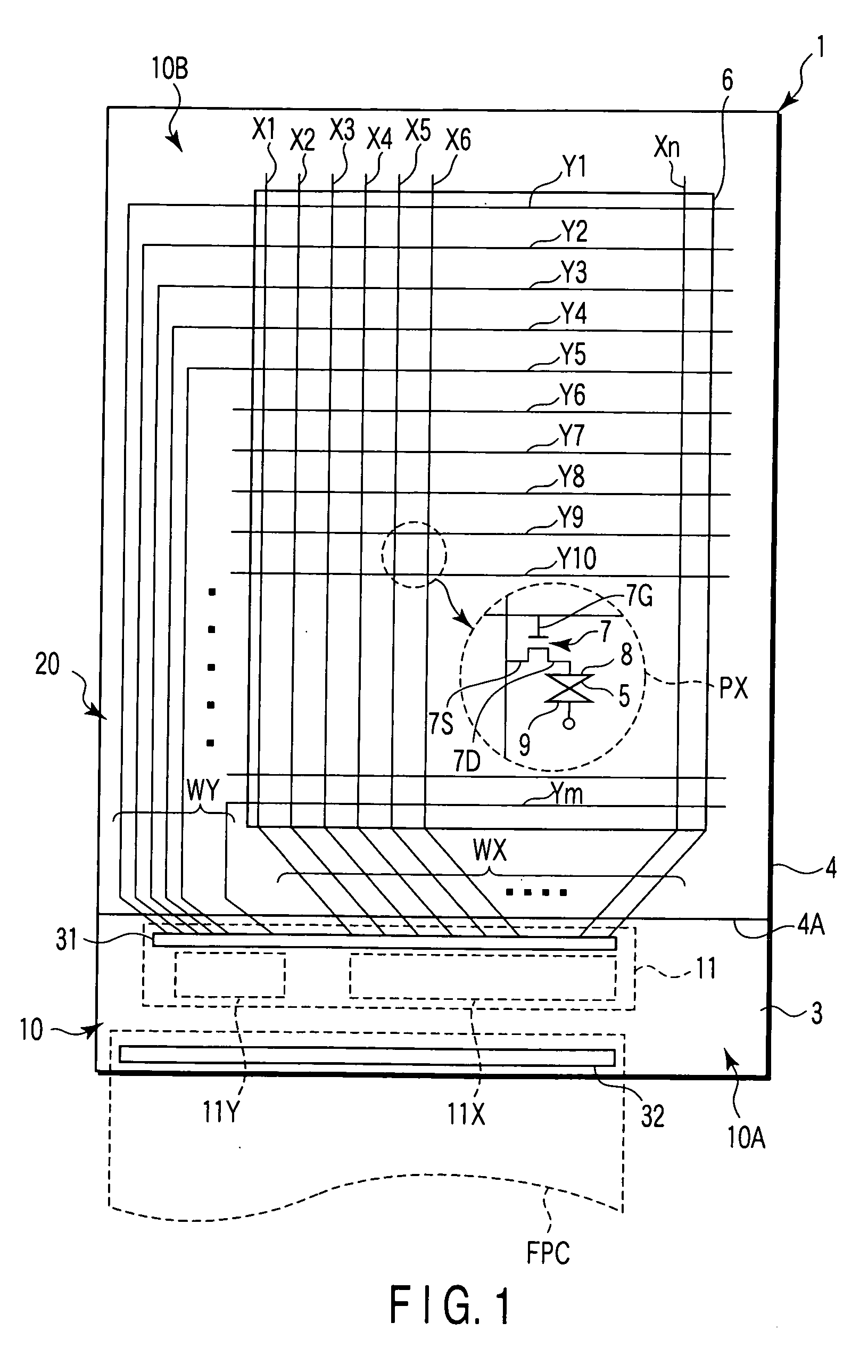
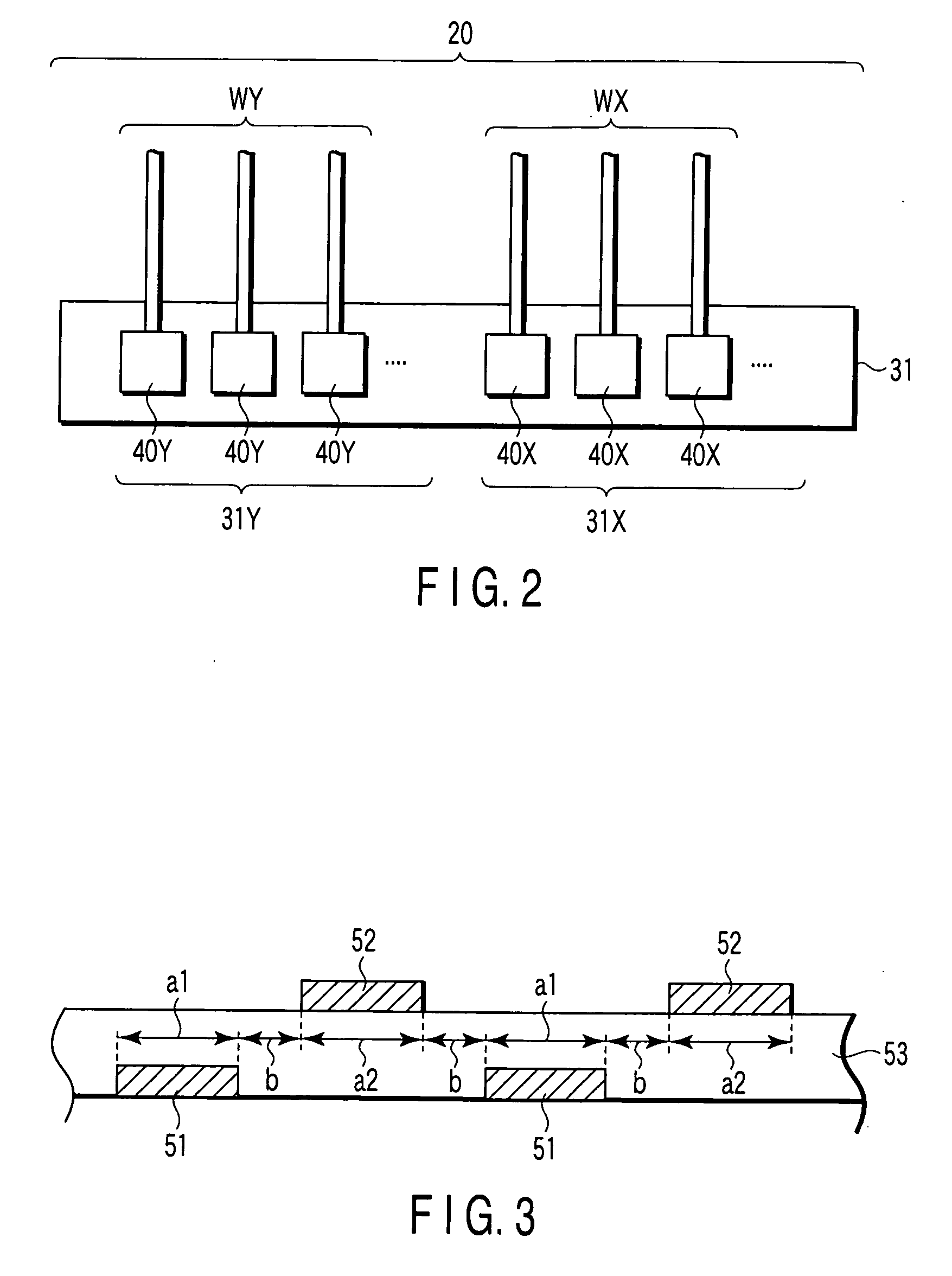
[0047] As is shown in FIG. 4, scan lines Y (1, 2, 3, . . . are disposed in the active area 6. The input sections 40Y (1, 2, 3, . . . ) and the connection wiring lines WY (1, 2, 3, . . . ), which connect the scan lines Y and the associated input sections 40Y, are disposed in the outer peripheral part 10. In the example shown in FIG. 4, even-numbered connection wiring lines WY (2, 4, . . . ) are disposed in the same layer as the scan lines Y. Odd-numbered connection wiring lines WY (1, 3, . . . ) are disposed in a layer different from the layer of the scan lines Y, for example, in the same layer as signal lines X (not shown). Needless to say, all scan lines Y in the active layer 6 are disposed in the same layer.

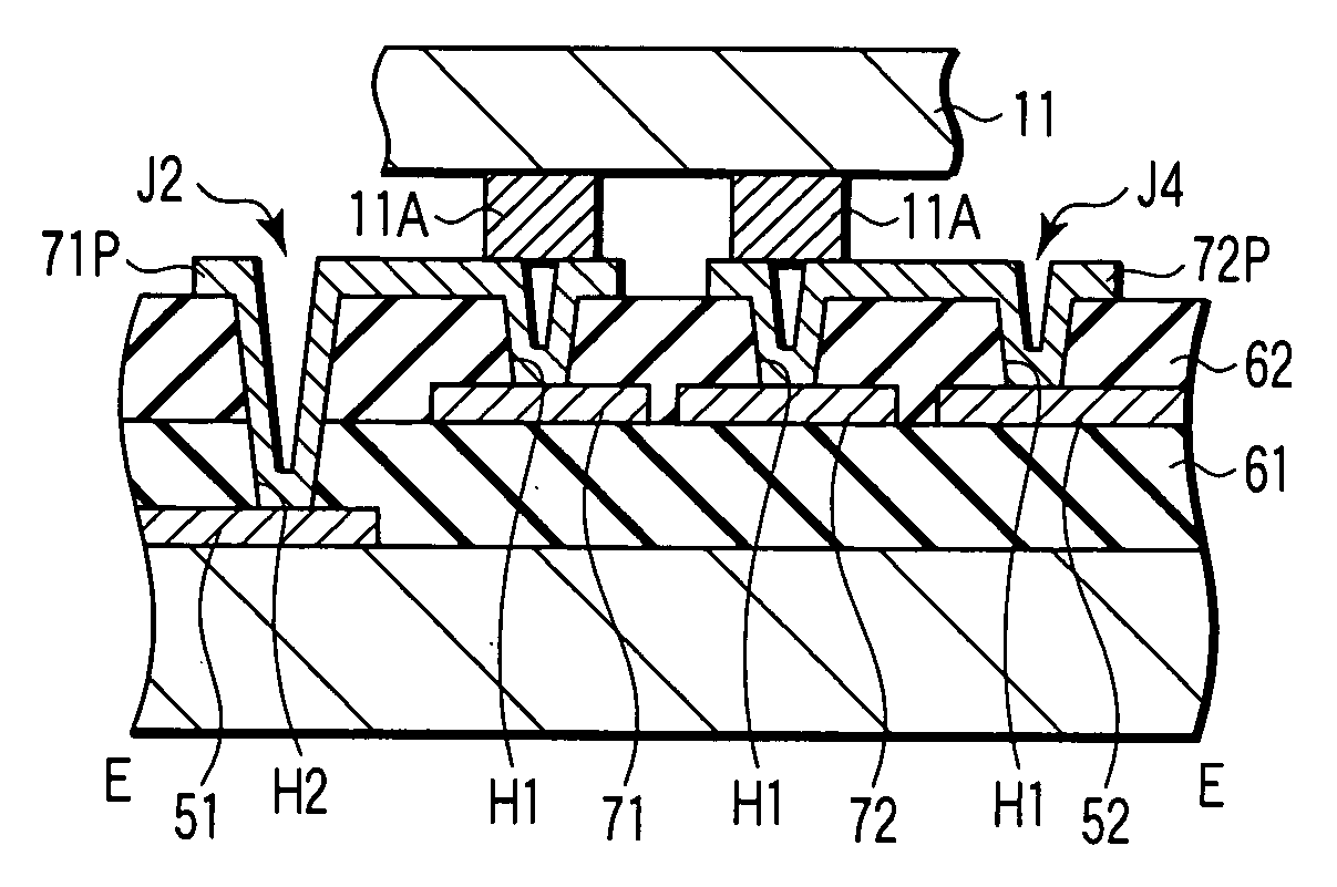
[0048] The connection wiring lines WY (2, 4, . . . ) are disposed in a lower layer than the connection wiring lines WY (1, 3, . . . ), and the insulating layer lies between the connection wiring lines WY (2, 4, . . . ) and the connection wiring lines WY (1, 3, . . . ) Specific...

embodiment 2

[0056] In Embodiment 2, the structural parts common to those in Embodiment 1 are denoted by like reference numerals, and a detailed description thereof is omitted.

[0057] As is shown in FIG. 7, scan lines Y (1, 2, 3, . . . ) are disposed in the active area 6. The input sections 40Y (1, 2, 3, . . . ) and the connection wiring lines WY (1, 2, 3, . . . ), which connect the scan lines Y and the associated input sections 40Y, are disposed in the outer peripheral part 10. In the example shown in FIG. 7, even-numbered connection wiring lines WY (2, 4, . . . ) are disposed in the same layer as the scan lines Y, and correspond to the first connection wiring lines 51 shown in FIG. 3. Odd-numbered connection wiring lines WY (1, 3, . . . ) are disposed in a layer different from the layer of the scan lines Y, and correspond to the second connection wiring lines 52 shown in FIG. 3. In short, the even-numbered connection wiring lines WY (2, 4, . . . ) and the odd-numbered connection wiring lines W...

embodiment 3

[0065] In Embodiment 3, the structural parts common to those in Embodiment 1 and Embodiment 2 are denoted by like reference numerals, and a detailed description thereof is omitted.

[0066] As is shown in FIG. 9A, scan lines Y (1, 2, 3, . . . ) are disposed in the active area 6. The input sections 40Y (1, 2, 3, . . . ) and the connection wiring lines WY (1, 2, 3, . . . ), which connect the scan lines Y and the associated input sections 40Y, are disposed in the outer peripheral part 10. In the example shown in FIG. 9A, even-numbered connection wiring lines WY (2, 4, . . . ) are disposed in the same layer as the scan lines Y, and correspond to the first connection wiring lines 51 shown in FIG. 3. Odd-numbered connection wiring lines WY (1, 3, . . . ) are disposed in a layer different from the layer of the scan lines Y, and correspond to the second connection wiring lines 52 shown in FIG. 3. In short, the even-numbered connection wiring lines WY (2, 4, . . . ) and the odd-numbered connec...


PUM


Abstract

A display device includes an active area that is composed of a plurality of pixels and a plurality of signal supply wiring lines that supply driving signals to the pixels, a plurality of input sections that are disposed outside the active area and function to input the driving signals that are to be supplied to the signal supply wiring lines, and a plurality of connection wiring lines that connect the signal supply wiring lines and the input sections. Mutually neighboring first connection wiring line and second connection wiring line of the connection wiring lines are disposed in different layers via an insulating layer.

Description

CROSS-REFERENCE TO RELATED APPLICATIONS [0001] This application is based upon and claims the benefit of priority from prior Japanese Patent Application No. 2004-378261, filed Dec. 27, 2004, the entire contents of which are incorporated herein by reference. BACKGROUND OF THE INVENTION [0002] 1. Field of the Invention [0003] The present invention relates generally to a display device, and more particularly to a display device including wiring lines that are arranged with high density on an outside peripheral part of an active area. [0004] 2. Description of the Related Art [0005] A display device, such as a liquid crystal display device, includes an active area that is composed of pixels arranged in a matrix. The active area includes a plurality of scan lines extending along rows of the pixels, a plurality of signal lines extending along columns of the pixels, switching elements that are disposed near intersections between the scan lines and signal lines, and pixel electrodes that are ...

Claims


Application Information

Patent Timeline
IPC IPC(8): G02F1/1345
CPCG02F1/133345G02F1/1345G02F2001/13456G02F1/13456
Inventor KIMURA, YOHEI
Owner TOSHIBA MATSUSHITA DISPLAY TECH
Why Eureka
Try Eureka