

Processes for forming layers for electronic devices using heating elements
- Summary
- Abstract
- Description
- Claims
- Application Information
AI Technical Summary
Benefits of technology
Problems solved by technology
Method used
Image

Examples
example 1
[0119] This Example demonstrates that a multiple pulsed signal for a heating element can be used to produce less heating compared to a continuous DC signal.
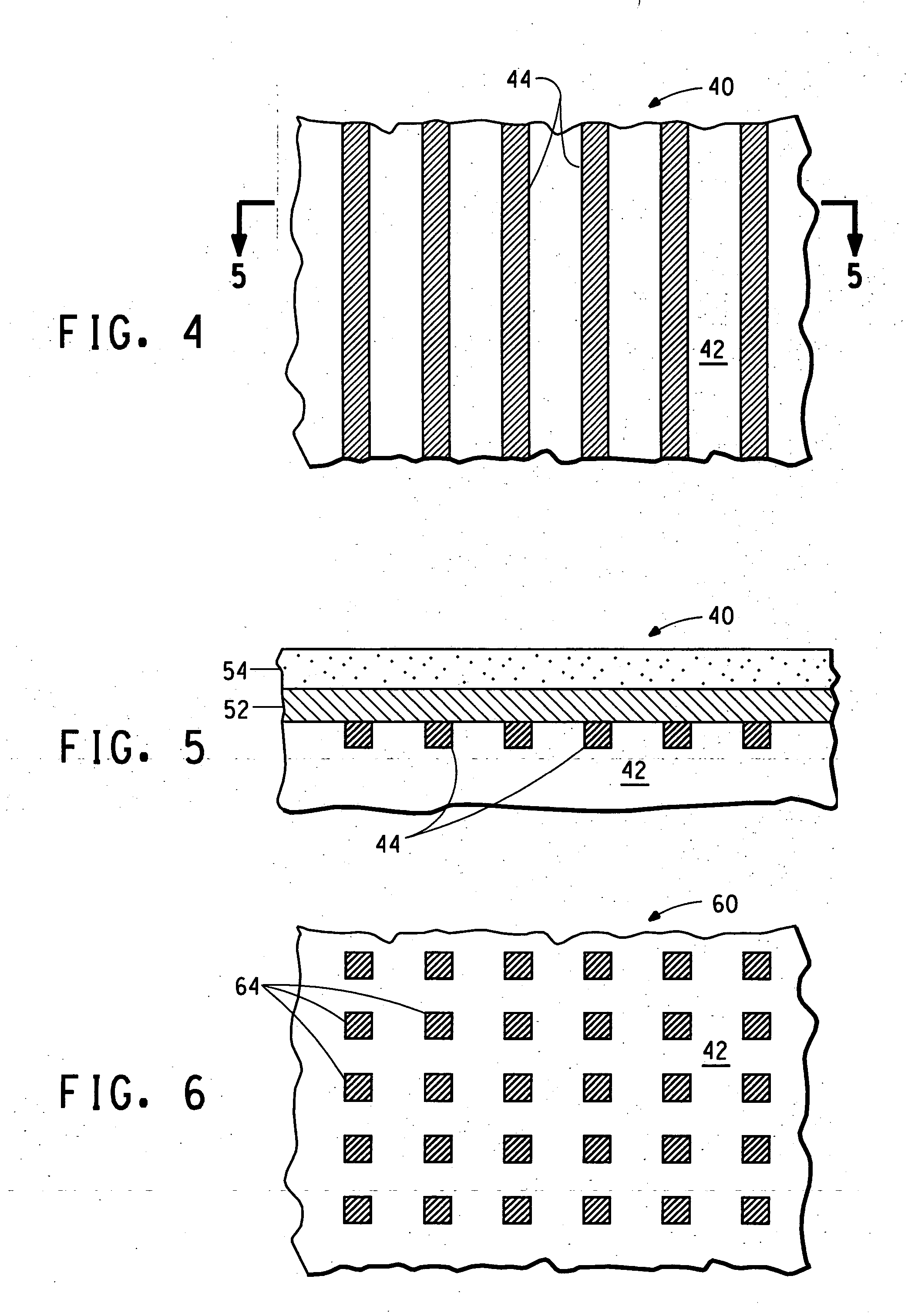
[0120] A micro-heater array 40 is designed and fabricated onto a glass substrate (i.e., base material 42) having a nominal thickness of 0.7 mm. The pattern of the micro-heater array 40 is similar to that shown in FIG. 4, wherein, from a plan view, the width and length of each heating element 44 (e.g. a strip) is approximately 85 microns and approximately 62 mm, respectively. The micro-heater array 40 is designed to fit a 4-inch (nominal) diagonal panel with 100 dots per inch in QVGA format (320×RGB×240 subpixels). The material used for heating elements 44 is ITO with a bulk resistivity of approximately 10−3 Ω-cm. The ITO is deposited by sputtering and patterned using a conventional photolithography technique. The thickness of the heating elements 44 is approximately 100 nm. The sheet resistance of each heating element 44 is appr...
example 2
[0122] This Example demonstrates that different materials can be used for the heating element of a multiple pulsed signal micro-heater array.
[0123] A micro-heater array 40 is designed and fabricated onto a glass substrate (i.e., base material 42) having a nominal thickness of 0.7 mm. The micro-heater array 40 has heating elements 44 with a pattern that is similar to that shown in FIG. 4, wherein, from a plan view, the width and length of each heating element 44 (e.g. a strip) is approximately 85 microns and approximately 62 mm, respectively. The micro-heater array 40 is designed to fit the 4-inch (nominal) diagonal panel with 100 dots per inch in QVGA format (320×RGB×240 subpixels). The material used for heating elements 44 is Cu with bulk resistivity of approximately 1.7×10⁻⁶ Ω·cm. The Cu is patterned using a conventional lithographic technique. The thickness of each heating element 44 (e.g., strip) is about 400 nm. The resistance of each heating element 44 is approximately 30 Ω. ...
PUM
 Abstract
Description
Claims
Application Information