Printed circuit board having three-dimensional spiral inductor and method of fabricating same

a printed circuit board and spiral inductor technology, applied in the direction of printed circuits, printed circuit components, inductances, etc., can solve the problems of insufficient inductance, difficult to form high inductance for a given size, and small size of current electronic devices, etc., to achieve high inductance

Active Publication Date: 2006-07-06
SAMSUNG ELECTRO MECHANICS CO LTD
View PDF5 Cites 64 Cited by
  • Summary
  • Abstract
  • Description
  • Claims
  • Application Information

AI Technical Summary

Benefits of technology

[0027] Therefore, the present invention has been made keeping in mind the above disadvantages occurring in the prior arts, and an object of the present invention is to provide a PCB having a three-dimensional spiral inductor, which assures high inductance in a small area of IC packages or PCBs of miniaturized and complicated electronic devices, and a method of fabricating the same.

Problems solved by technology

Meanwhile, current electronic devices are becoming small, light, and slim, and advances in fabrication and design technologies of the electronic devices promote miniaturization of the passive components used in the electronic devices.
However, the inductor is mainly fabricated in one of the three types shown in FIG. 1 because of spatial limitations.
However, the meander line inductor is disadvantageous in that since mutual inductances are generated in opposite directions and thus offset each other, it is difficult to form high inductance for a given size.
Of the three types of inductor, the spiral inductor is most advantageous, but is problematic in that the two-dimensional spiral inductor occupies too large an area of the substrate to be applicable to miniaturized and complicated electronic current devices while insufficient inductance is assured.
However, in the above prior arts, even though the spiral inductor is most advantageous, the spiral inductor is problematic in that it occupies too large an area of a substrate to be applied to miniaturized and complicated current electronic devices, and thus insufficient inductance is assured.

Method used


Image

  • Printed circuit board having three-dimensional spiral inductor and method of fabricating same
  • Printed circuit board having three-dimensional spiral inductor and method of fabricating same
  • Printed circuit board having three-dimensional spiral inductor and method of fabricating same

Examples


Embodiment Construction

[0049] Hereinafter, a detailed description will be given of a PCB having a three-dimensional spiral inductor and a method of fabricating the same according to the present invention, with reference to the drawings.

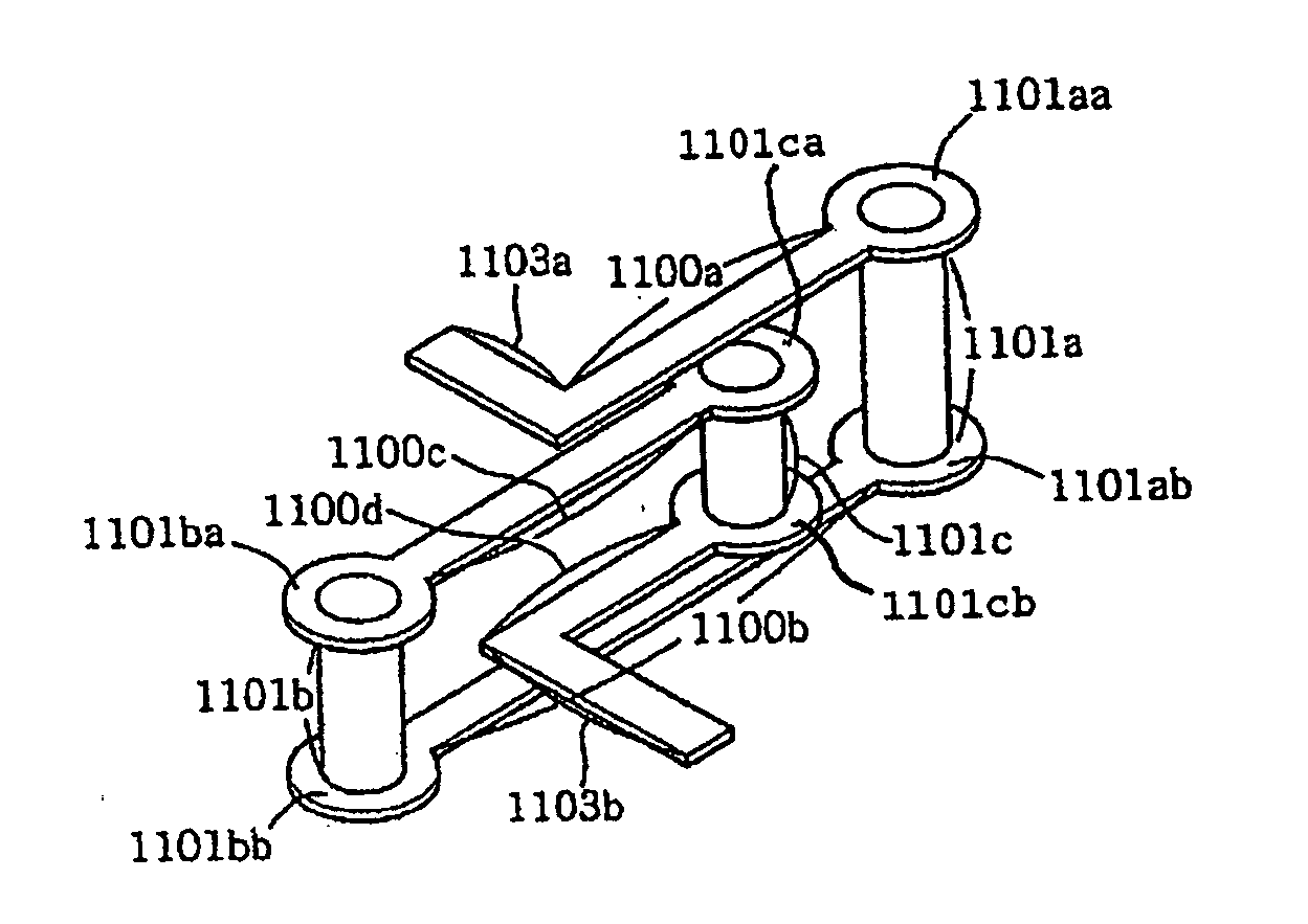
[0050]FIG. 10 is a perspective view of a four-layered three-dimensional inductor, which is used in a PCB comprising the three-dimensional spiral inductor according to an embodiment of the present invention.

[0051] Referring to FIG. 10, the three-dimensional inductor, which is used in the PCB having the three-dimensional spiral inductor according to an embodiment of the present invention, is provided with a plurality of coil conductor patterns 1100a-1100d, a plurality of coil via holes 1101a-1101c, and two lead out patterns 1103a, 1103b. Land parts 1101aa and 1101ab, 1101ba and 1101bb, and 1101ca and 1101cb are formed on both ends of the coil via holes 1101a-1101c.

[0052] In FIG. 10, the coil conductor patterns 1100a-1101d are shaped in a micro-strip, and separated and para...


PUM

PropertyMeasurementUnit
external poweraaaaaaaaaa
conductiveaaaaaaaaaa
lengthaaaaaaaaaa

Abstract

A printed circuit board (PCB) having a three-dimensional spiral inductor, which includes a plurality of insulating layers and conductor layers. The PCB comprises a plurality of coil conductor patterns made of conductive material and shaped into strips, which is provided on the plurality of conductor layers, respectively, such that the plurality of coil conductor patterns are parallel to each other and positioned on the same plane perpendicular to the conductor layers, and in which each of the plurality of coil conductor patterns is longer than an adjacent inner coil conductor pattern.

Description

INCORPORATION BY REFERENCE [0001] The present application claims priority under 35 U.S.C. §119 to Korean Patent Application No. 2004-116806 filed on Dec. 30, 2004. The content of the application is incorporated herein by reference in its entirety. BACKGROUND OF THE INVENTION [0002] 1. Field of the Invention [0003] The present invention relates, in general, to a printed circuit board (PCB) having an inductor and a method of fabricating the same and, more particularly, to a PCB having an inductor, in which the inductor is formed by appropriately arranging spiral vertical structures so as to effectively use the space of the PCB, and a method of fabricating the same. [0004] 2. Description of the Prior Art [0005] Used in electric and electronic circuits, a passive component is generally classified into a resistor, a capacitor, and an inductor. Of them, the capacitor and the inductor are the most basic components capable of storing and supplying energy. Since they have frequency character...

Claims


Application Information

Patent Timeline
Patent Type & Authority Applications(United States)
IPC IPC(8): H01F5/00
CPCH01F17/0006H01F17/0033H01F2017/002H05K1/165H05K3/4602H05K3/4652H05K2201/09536H05K2201/0959H05K2201/097H05K1/16H01F5/00
Inventor KIM, HANMIN, BYOUNG YOULKIM, YOUNG WOOLEE, YOUNG JAERYU, CHANG MYUNG
Owner SAMSUNG ELECTRO MECHANICS CO LTD
Why Eureka
Try Eureka