Wafer-processing tape and method of producing the same

a processing tape and processing method technology, applied in the field of wafer processing tape, can solve the problems of increasing production cost, complex technical complexity, and consequently, and it is difficult to distinguish between untreated and treated portions processed only by corona treatmen

Active Publication Date: 2006-07-13
FURUKAWA ELECTRIC CO LTD
View PDF11 Cites 41 Cited by
  • Summary
  • Abstract
  • Description
  • Claims
  • Application Information

AI Technical Summary

Benefits of technology

[0032] adhering directly the removable adhesive layer side of the tape (c) and the adhesive layer side of the tape (d), thereby producing a composite wafer-processing tape;

Problems solved by technology

However, the adhesive agent layer (or the removable adhesive or adhesion agent layer) is easily separated or peeled off from the removable adhesive agent layer (or the base film) by weak force, leaving the adhesive agent (or the removable adhesive or adhesion agent) adhered to the ring frame, i.e. adhesive residue.
As a result, in the wafer-processing tapes that can be used in such an application, the portion in contact with the ring frame demands special processing, such as alteration of the adhesive agent (or the removable adhesive or adhesion agent) or alteration of surface-modification conditions of the base film, and / or special tape structure, leading to technical complexity and consequently increased production cost.
Although the corona treatment is generally applicable to a wide variety of films independent of the kind of the base film, the boundary of the treated portion is not distinct, and thus, it is difficult to distinctly distinguish untreated and treated portions processed only by corona treatment.
On the other hand, in the primer treatment, it is necessary to select a suitable primer material according to the material of the base film to be used, and when a polyolefin-series film is used, it is generally difficult to keep the adhesive strength between the base film and the primer on a high level, often resulting in peeling-off between the primer layer and the base film when the wafer-processing tape is removed from the ring frame, and hence occurrence of adhesive residue on the ring frame.
To control the peeling force of the removable adhesive layer, it is necessary, for example, an additional step of altering the removable adhesive to be used, making the process very complicated.

Method used


Image

  • Wafer-processing tape and method of producing the same
  • Wafer-processing tape and method of producing the same
  • Wafer-processing tape and method of producing the same

Examples


example 1

[0071] To a solvent of toluene 400 g, a mixed solution of n-butyl acrylate 128 g, 2-ethylhexyl acrylate 307 g, methyl methacrylate 67 g, methacrylic acid 1.5 g, and benzoylperoxide as a polymerization initiator was added, dropwise, in an appropriately adjusted addition rate, followed by reaction of these by appropriately adjusting a reaction temperature and a reaction time, to give a solution of a polymer compound (1) having a given functional group.

[0072] Then, to the thus-obtained solution, added were, dropwise, a compound (2) having a radiation-curable carbon-carbon double bond and a given functional group, which was 2.5 g of 2-hydroxyethyl methacrylate separately synthesized from methacrylic acid and ethylene glycol, and hydroquinone as a polymerization inhibitor, followed by reaction of these, to give a solution of a compound (A) having a radiation-curable carbon-carbon double bond. Then, to 100 mass parts of the compound (A) in the thus-obtained compound (A) solution, was add...

example 2

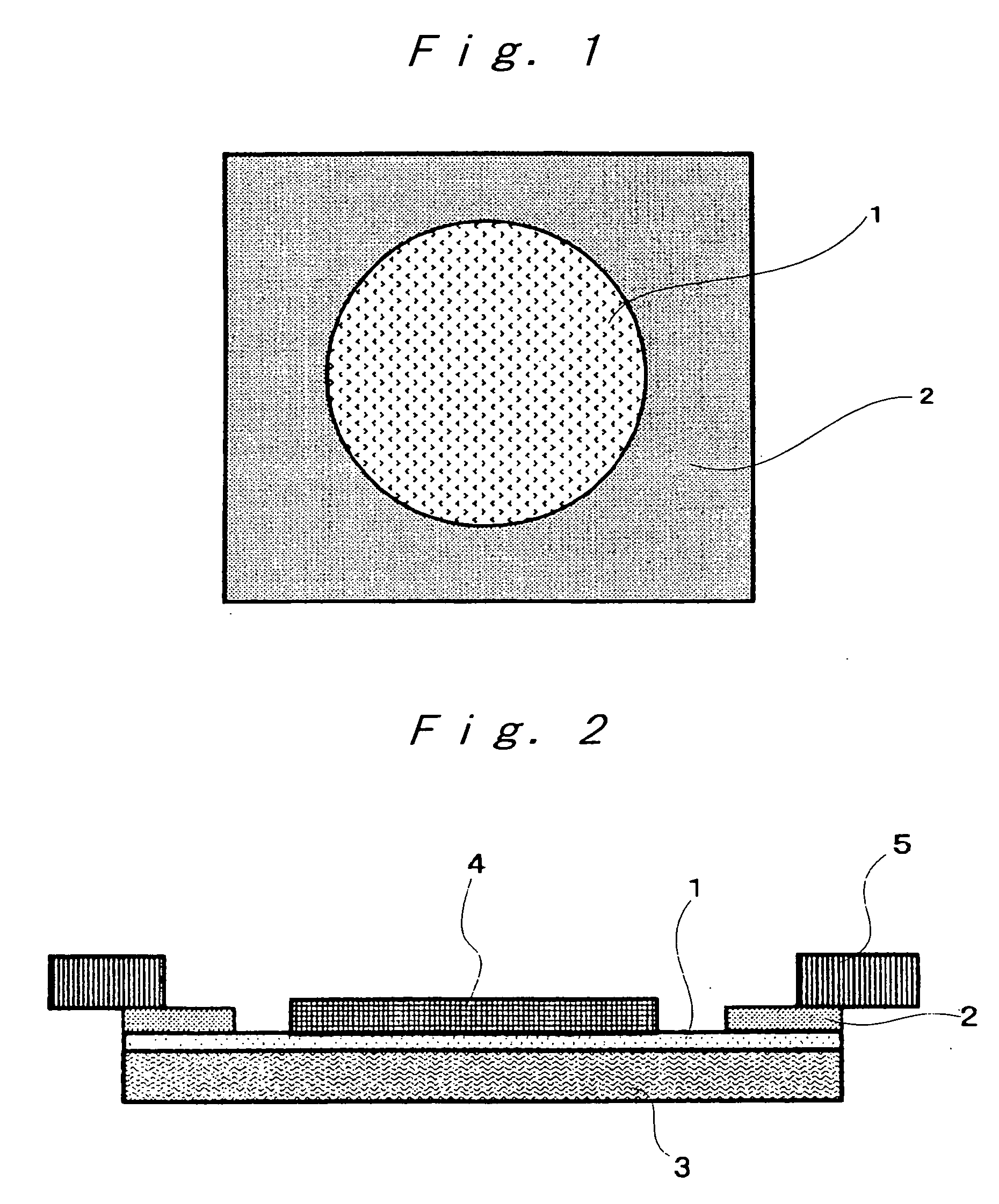
[0089] A wafer-processing tape was prepared in the same manner as in Example 1 by using the materials and the preparation method similar to Example 1, except that the removable adhesive layer was prepared from a material in which the removable adhesive components of Example 1 was added with 0.5 parts by mass of a coloring agent (Kayaset Blue N (trade name), manufactured by Nippon Kayaku).

[0090] By using the wafer-processing tape, a silicon wafer of 8 inches (20.32 cm) in diameter was mounted on a stainless steel ring frame in the same manner as in Example 1. During the mounting, the portion having the removable adhesive layer in the wafer-processing tape was colored, allowing the mounting process to be carried out easily and assuredly. Then, after the silicon wafer was diced; the chips were picked up; and the wafer-processing tape used was peeled off from the ring frame. It was confirmed that there was no adhesive residue on the ring frame in observation with the naked eye. At that...

example 3

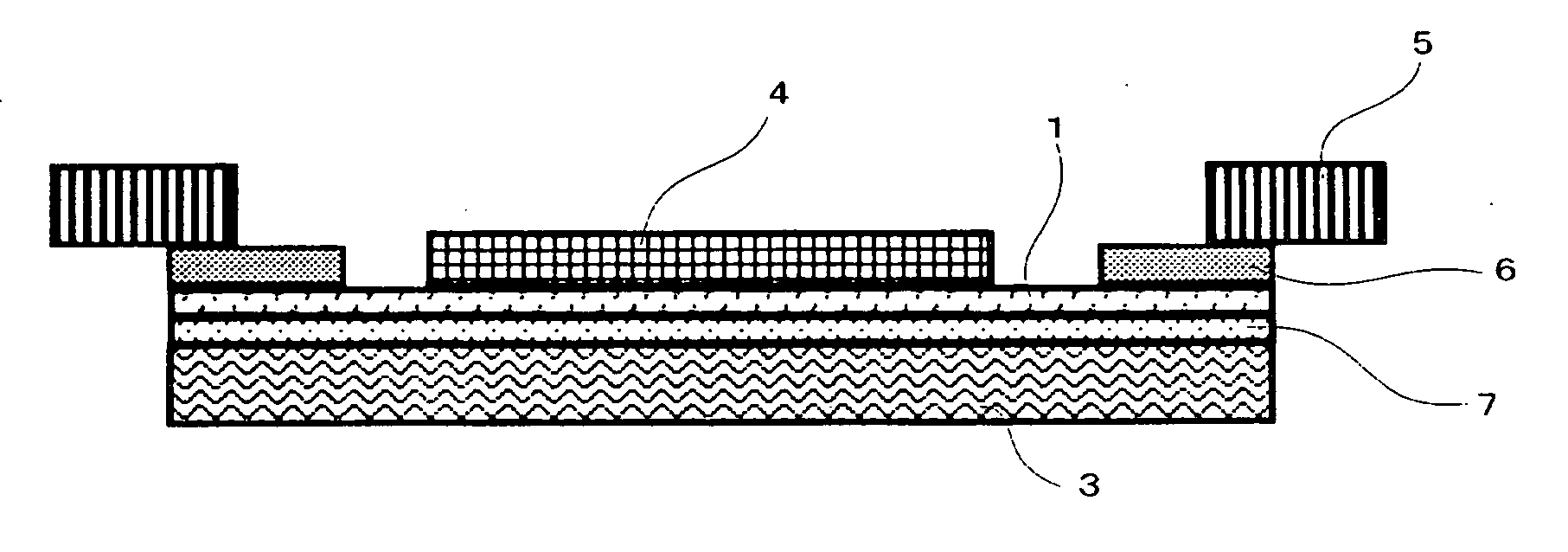
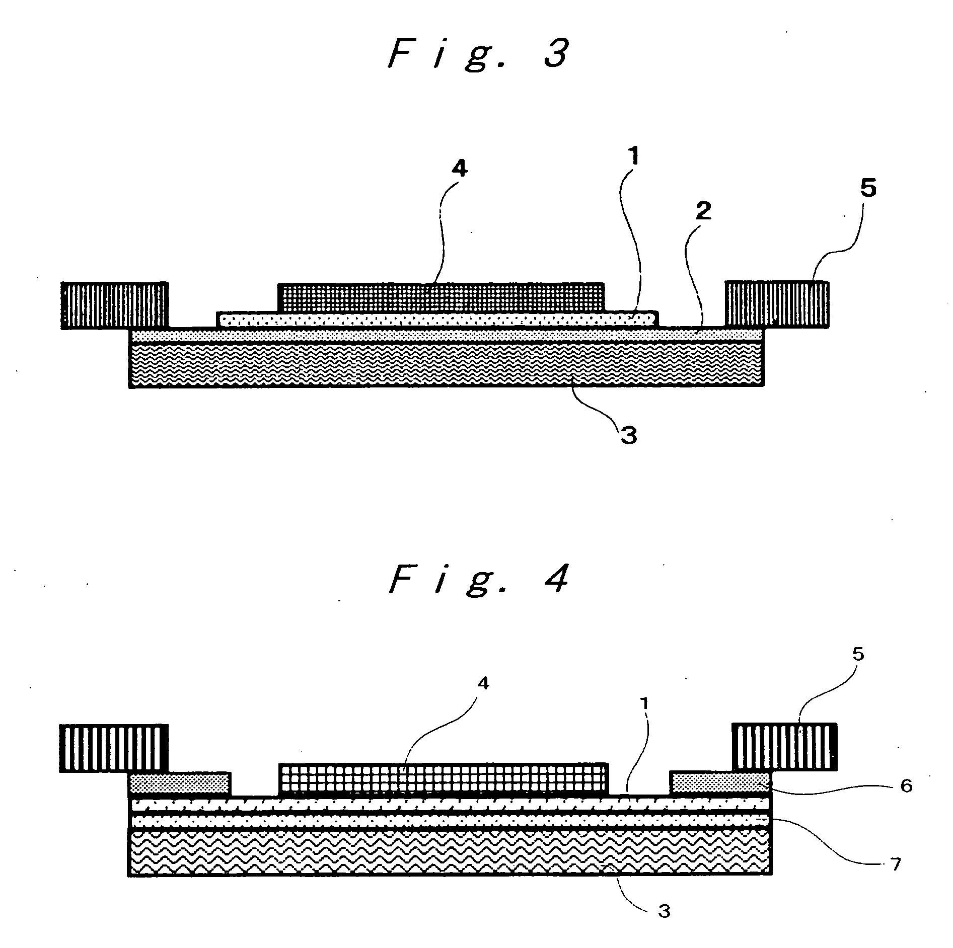
[0091] The wafer-processing tape of Example 3 was prepared, using the base film, the adhesive agent, the removable adhesive or adhesion agent, and the separator film similar to those in Example 1. However, the wafer-processing tape in Example 1 had the structure of the base film, the removable adhesive or adhesion layer, the removable adhesive layer, and the separator film in that order, but the wafer-processing tape in Example 3 had the structure of the base film, the removable adhesive layer, the removable adhesive or adhesion layer, and the separator film in that order.

[0092] That is, a removable adhesive layer tape (c) having a removable adhesive layer with thickness 5 μm was obtained, by preparing a composition obtained by blending the removable adhesive components similar to those of Example 1, applying the composition onto a corona-treated polyolefin-series base film of thickness 100 μm, and drying the coated film under heating.

[0093] Then, the middle portion of a PET-serie...


PUM

PropertyMeasurementUnit
thicknessaaaaaaaaaa
thicknessaaaaaaaaaa
thicknessaaaaaaaaaa

Abstract

A wafer-processing tape, which has an adhesive layer (1) and a removable adhesive layer (2) formed on a surface of a base film (3), and which has an area where B>A, and an area where A>B, in which a peeling force between the base film (3) and the adhesive layer (1) is designated as A, and peeling forces between a target to be bonded (4) and the adhesive layer (1) and between a target to be bonded (5) and the removable adhesive layer (2) are designated as B, wherein the adhesive layer (1) is transferred onto the chip side during pickup in the area where B>A, and the removable adhesive layer (2) is not transferred onto the target to be bonded (5) in the area where A>B during peeling off the tape.

Description

TECHNICAL FIELD [0001] The present invention relates to a wafer-processing tape at least having an adhesive layer formed on a base film. BACKGROUND ART [0002] An assembling process of a semiconductor device, such as an IC or the like, comprises the steps of: cutting and separating (dicing) a semiconductor wafer and the like into respective chips, after patterning; mounting the chips on a substrate or the like; and sealing them with a resin or the like. [0003] In the dicing step, a semiconductor wafer is adhered, and thus fixed, to a wafer-processing tape in advance, and then it is diced into the shape of chip. In the subsequent mounting step, the diced chip, having a removable adhesive or adhesion agent that is contained in a removable adhesive or adhesion layer separable from the base film, is peeled off (picked up) from the base film, and then fixed, for example, to a substrate by the removable adhesive or adhesion agent for adhering and fixing, which agent has adhered to the chip...

Claims


Application Information

Patent Timeline
Patent Type & Authority Applications(United States)
IPC IPC(8): D02G3/00C09J7/38H01L21/301H01L21/58H01L21/68
CPCC09J7/0207Y10T428/2809C09J2201/36C09J2203/326H01L21/6836H01L24/27H01L24/83H01L2221/68327H01L2224/274H01L2224/83191H01L2224/8385H01L2924/01002H01L2924/01005H01L2924/01013H01L2924/01015H01L2924/01033H01L2924/01074H01L2924/01079H01L2924/01082H01L2924/07802H01L24/29H01L2224/2919H01L2924/01006H01L2924/01019H01L2924/01055H01L2924/0665C09J2201/28Y10T428/28Y10T428/287Y10T428/2848Y10T428/298Y10T428/2891H01L2924/10253H01L2924/00H01L2924/12044C09J7/38C09J2301/204C09J2301/208H01L21/30H01L21/50H01L21/48H01L21/78
Inventor KITA, KENJIMORISHIMA, YASUMASAISHIWATA, SHINICHI
Owner FURUKAWA ELECTRIC CO LTD
Why Eureka
Try Eureka