Front plante for plasma dispay and plasma display

a plasma display and front panel technology, applied in the field of front panel for plasma display, can solve problems such as increasing costs, and achieve the effect of high-visibility imag

Inactive Publication Date: 2006-07-13
DAI NIPPON PRINTING CO LTD
View PDF3 Cites 30 Cited by
  • Summary
  • Abstract
  • Description
  • Claims
  • Application Information

AI Technical Summary

Benefits of technology

[0037] According to the present invention, there is provided a plasma display that is shielded so as not to emit electromagnetic waves, near infrared rays, and light with specific wavelengths originating from the emission spectrum of an insert gas, that can display an image with a color tone adjusted according to customer's preference, and that can display a highly visible image owing to the property of preventing reflection of extraneous light and the anti-glare properties imparted.

Problems solved by technology

These techniques are disadvantageous in that they demand additional steps for the formation of the terminal areas, and also facilities and materials for use in the additional steps, which leads to an increase in costs.

Method used


Image

  • Front plante for plasma dispay and plasma display
  • Front plante for plasma dispay and plasma display
  • Front plante for plasma dispay and plasma display

Examples


example 1

(Preparation of Electromagnetic Wave Shielding Layer)

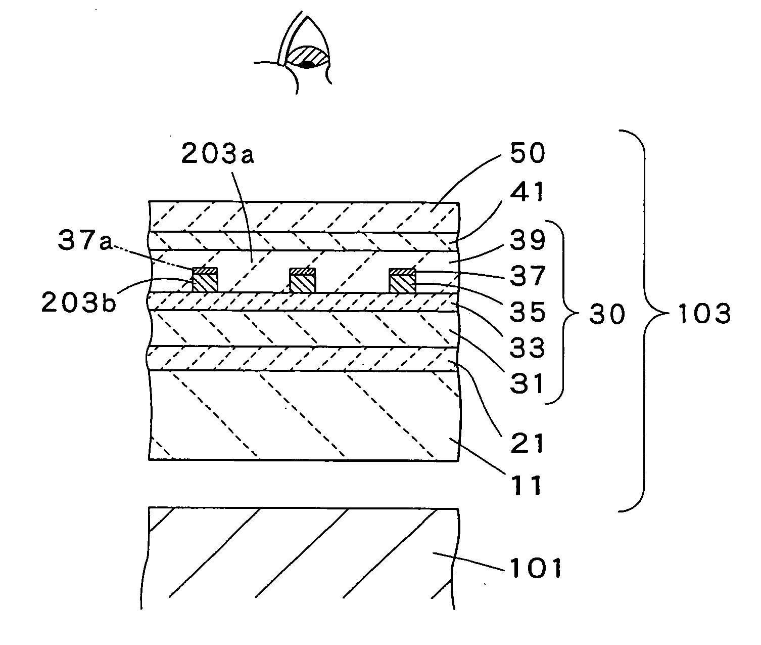
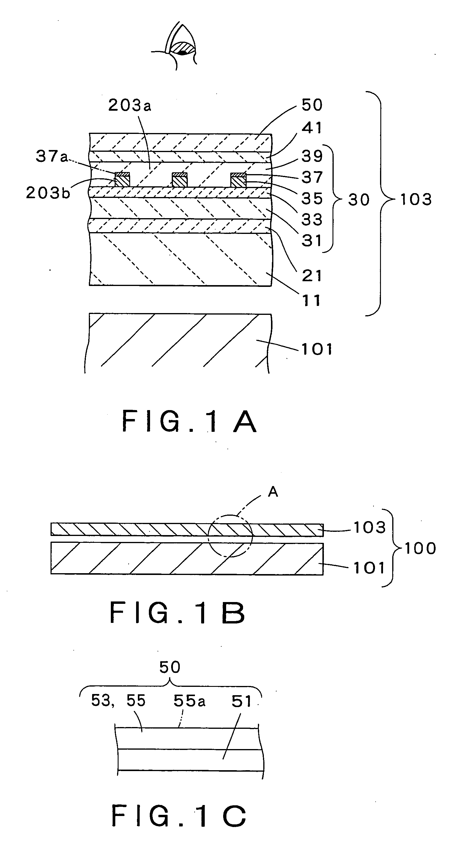
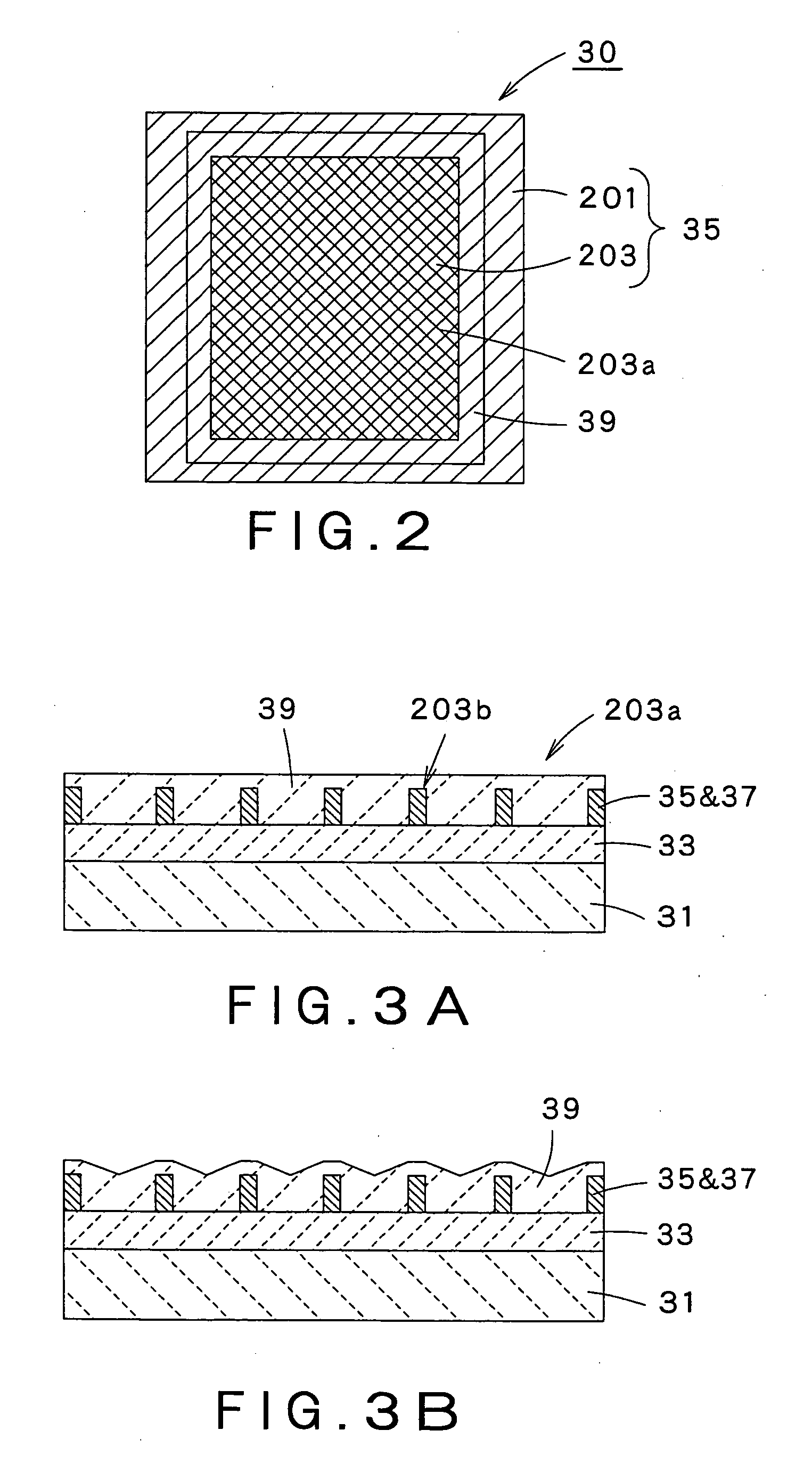
[0122] A biaxially oriented PET film A4300 (trademark, polyethylene terephthalate manufactured by Toyobo Co., Ltd., Japan) with a thickness of 100 μm, serving as the transparent substrate film, and electrolytic copper foil with a thickness of 10 μm, serving as the metal layer, were laminated with the second transparent adhesive layer made from a two-part curing urethane adhesive, and this was aged at 50° C. for 3 days, thereby obtaining a laminate. For the adhesive, polyester urethane polyol was used as the main agent, and xylene diisocyanate was used as the curing agent. The adhesive was applied in such an amount that the dry adhesive layer would have a thickness of 4 μm. A mesh part was photolithographically made in the copper foil in this laminate. Using the existing production line for shadow masks for color TV, the laminate in the form of a belt-shaped (rolled-up) continuous web was subjected to a series of the steps of fro...

example 2

[0125] A front panel for plasma display was obtained in the same manner as in Example 1, except that PS Violet RC (trademark, manufactured by Mitsui Toatsu Dyes, Ltd., Japan) was further added, as the coloring agent for color tone adjustment, to the composition liquid for forming the smoothing resin layer in an amount (dry basis) of 0.109 g / m2.

example 3

[0126] A front panel for plasma display was obtained in the same manner as in Example 1, except that the four coloring agents used in Example 1 were incorporated in the third transparent adhesive layer and that no coloring agent was incorporated in the smoothing resin layer.


PUM

PropertyMeasurementUnit
shielding efficiencyaaaaaaaaaa
frequenciesaaaaaaaaaa
wavelengthsaaaaaaaaaa

Abstract

A front panel for plasma display comprises a transparent substrate 11 and an electromagnetic wave shielding layer 30 provided on one surface of the transparent substrate 11 through a first transparent adhesive layer 21. The electromagnetic wave shielding layer 30 comprises a transparent substrate film 31, a metal layer 35 that includes a mesh part203 and a frame part 201 surrounding the mesh part 203, and a smoothing resin layer 39. On the metal layer 35 is provided a blackening treatment layer 37. A third transparent adhesive layer 41 and a transparent protective layer 50 are laminated in this order to the electromagnetic wave shielding layer 30. The smoothing resin layer 39 and/or the third transparent adhesive layer 41 contains a near infrared rays absorbing agent and a coloring agent for color tone correction.

Description

FIELD OF THE INVENTION [0001] The present invention relates to a front panel for a plasma display, and more particularly, to a front panel for a plasma display that is mounted on the front of a plasma display element (also referred to as a PDP) so as to shield electromagnetic waves and near infrared rays that are emitted from the element and also to make an image displayed on a display (also referred to as an image display) highly visible. BACKGROUND ART [0002] 1. Background of the Invention [0003] A PDP is composed of a glass substrate having a data electrode and a fluorescent layer, and a glass substrate having a transparent electrode, with a gas such as xenon or neon being sealed in a space between the two glass substrates. PDPs can be made large in screen size as compared with conventional CRT-TVs and have come to be used widely. In operation, a PDP produces, as unwanted radiation, large amounts of electromagnetic waves, near infrared rays, and unwanted light with specific wavel...

Claims


Application Information

Patent Timeline
Patent Type & Authority Applications(United States)
IPC IPC(8): B32B15/04G02B5/20H01J17/16H05K9/00
CPCB32B15/04G02B5/208H01J11/44H01J2211/446H05K9/0096Y10T428/31678H01J2211/448B32B15/08B32B2305/38B32B2307/212B32B2307/4026B32B2307/412B32B2457/204
Inventor NAITO, NOBUOARAKAWA, FUMIHIROMASAKI, TADAHIRO
Owner DAI NIPPON PRINTING CO LTD
Why Eureka
Try Eureka