Display element and image display device

a technology of display element and image display device, which is applied in the direction of photomechanical treatment, identification means, instruments, etc., can solve the problems of low light utilization efficiency of light from the illuminating light source, disadvantageous in its large power consumption, and complex structure, and achieves low cost, simple structure, and high visible image

Inactive Publication Date: 2005-07-14
FUJIFILM CORP +1
View PDF1 Cites 2 Cited by
  • Summary
  • Abstract
  • Description
  • Claims
  • Application Information

AI Technical Summary

Benefits of technology

[0005] The present invention has been made to solve the above problems and has an object to provide a display element and an image display device with a simple structure at low cost, which are capable of displaying a highly visible image, easily switching ON / OFF of color display, and increasing a size of a screen.

Problems solved by technology

In addition, the utilization efficiency of light from the illuminating light source is low.
Therefore, the liquid crystal display is disadvantageous in its large power consumption, the necessity of electric power for displaying an image, its small viewing angle and the like.
However, the display device for making control as to whether to fill the colored liquid or not for each cell as disclosed in JP 05-241515 A has a problem that the structure is complicated.
Furthermore, the systems as disclosed in JP 09-44107 A, JP 09-311654 A and JP 10-260651 A are disadvantageously incapable of forming a clear image and retaining a formed image.
Moreover, the system as disclosed in JP 10-39799 A is disadvantageous in that the size of a screen is hardly increased and its structure is complicated.

Method used


Image

  • Display element and image display device
  • Display element and image display device
  • Display element and image display device

Examples


first embodiment

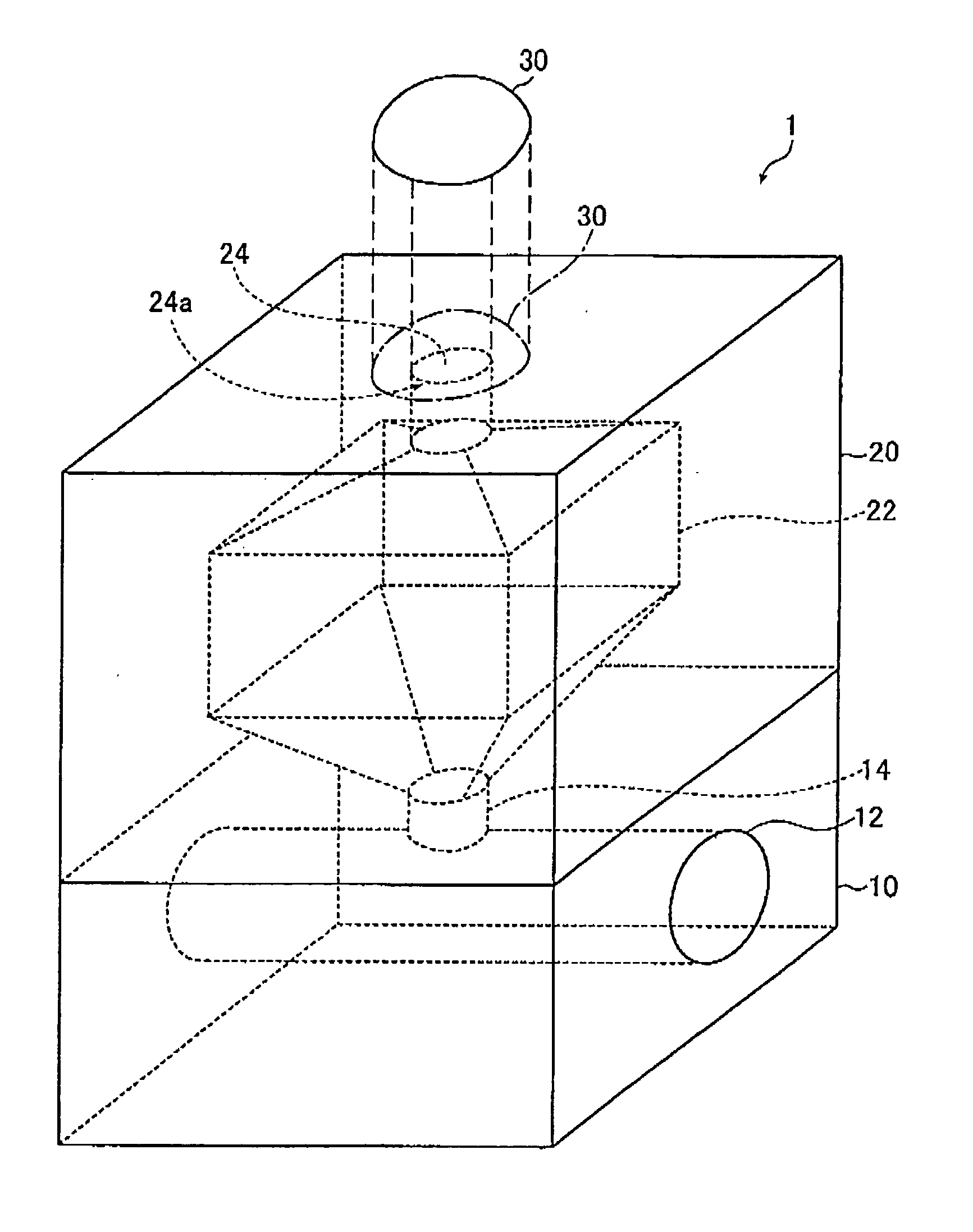
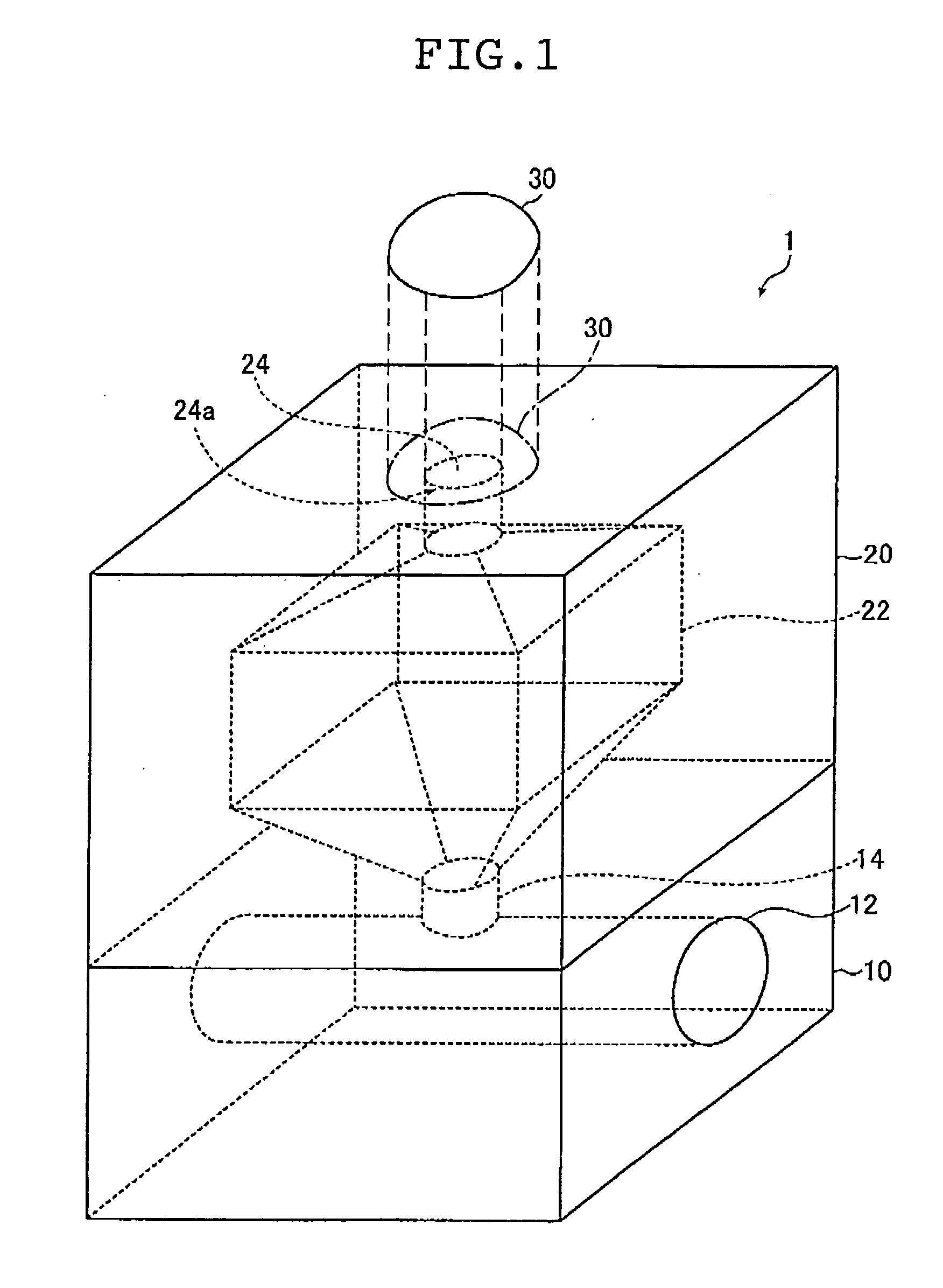
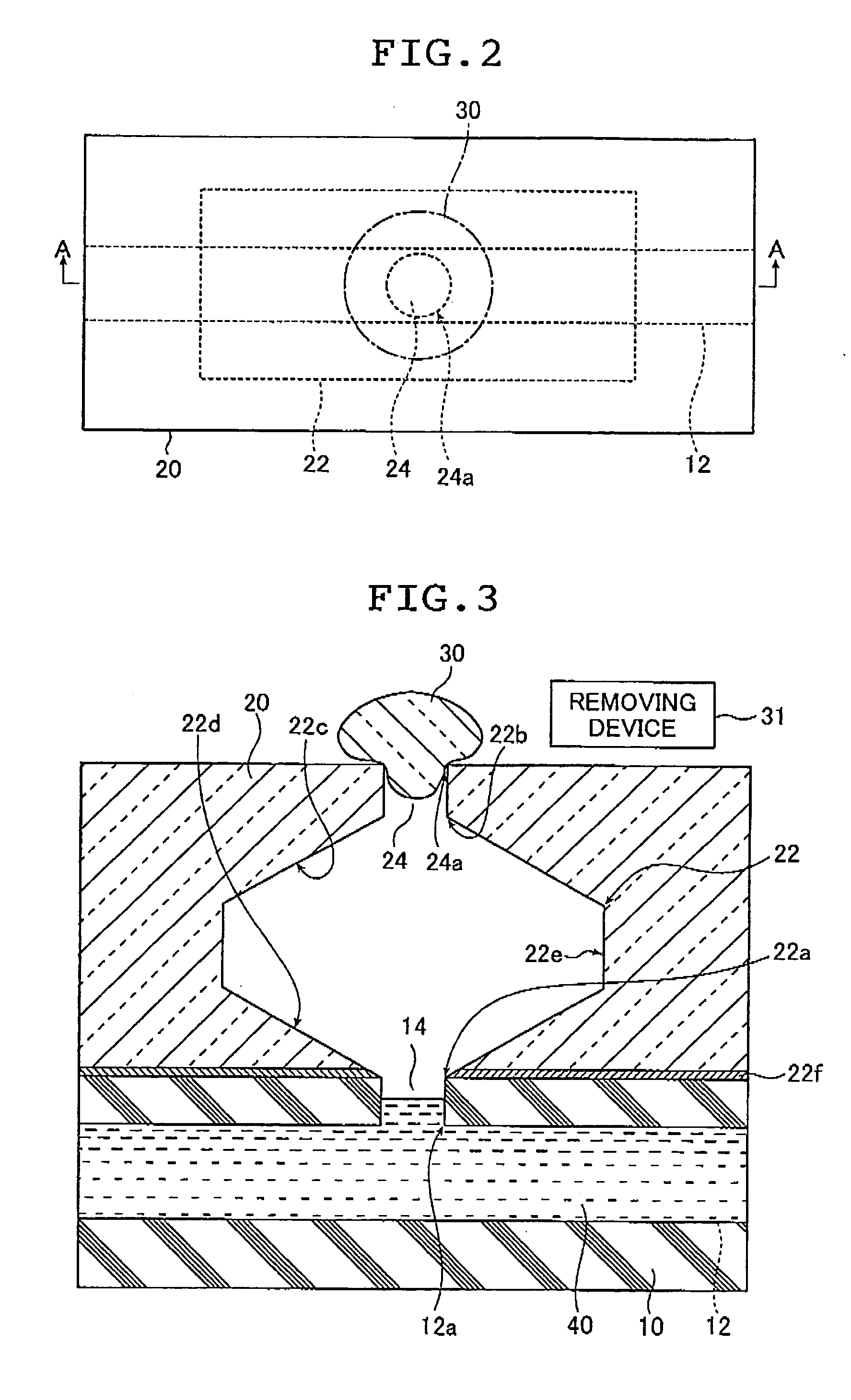
[0030] Hereinafter, a display element according to a first embodiment of the present invention will be described. FIG. 1 is a perspective view showing a display element 1 according to the first embodiment. FIG. 2 is a plan view showing the display element 1, and FIG. 3 is a vertical sectional view of the display element 1 taken along a plane perpendicular to a paper plane, passing through a line A-A in FIG. 2.

[0031] As shown in FIGS. 1 to 3, in the display element 1 according to the first embodiment, a transparent substrate 20 is provided on a support substrate 10 made of a material having a light-shielding property. In the support substrate 10, an ink supply passage 12 is provided in a direction along a surface of the support substrate 10, that is, a horizontal direction in FIGS. 2 and 3. In the approximate center of the transparent substrate 20, an image display section 22 forming a void space is provided. The shape of the image display section 22 is not particularly limited. As ...

second embodiment

[0055] A second embodiment of the present invention will now be described. In this second embodiment, a plurality of the display elements 1 according to the first embodiment are arranged to form a display unit. Then, a plurality of the thus formed display units are arranged in a matrix to form an image display device. FIG. 5 shows a schematic structure of an image display device 100 according to the second embodiment. As illustrated in FIG. 5, a plurality of display units are arranged in a matrix on a substrate 102 in the image display device 100. For each of the display units, a plurality of the display elements 1 described above, for example, three display elements are arranged so as to be adjacent to each other.

[0056] A small circle B shown in FIG. 5 is a partially enlarged view of-one of the display units arranged in the image display device 100. As shown in the small circle B shown in FIG. 5, each of the display units is composed of three display elements 1001a, 1001b and 1001...

third embodiment

[0065] Hereinafter, a display element according to a third embodiment of the present invention will be described. FIG. 6 is a perspective view showing a display element 2 according to the third embodiment of the present invention. FIG. 7 is a plan view of the display element 2, and FIG. 8 is a vertical sectional view showing a cross section of the display element 2 cut along a plane perpendicular to the paper plane and passing through a line B-B of FIG. 7.

[0066] As shown in FIGS. 6 to 8, in the display element 2 according to this third embodiment, a transparent substrate 60 is provided on a support substrate 50 formed of a material having a light-shielding property. In the support substrate 50, an ink supply passage 52, through which an ink flows unidirectionally, is provided in a direction along a surface of the support substrate 50, that is, in a horizontal direction as shown in FIGS. 7 and 8.

[0067] An image display section 62 having a space is formed between an upper surface of...


PUM

PropertyMeasurementUnit
thicknessaaaaaaaaaa
thicknessaaaaaaaaaa
thicknessaaaaaaaaaa

Abstract

A display element for displaying an image with an ink has an transparent substrate having a void space for containing the ink therein to form a display section. The space has the first opening and the second opening opposing to each other. The first opening communicates with an atmosphere via an atmosphere communicating passage. The second opening allows the ink to introduce to the space of the image display section from an ink supply passage. The atmosphere communicating passage is controlled to close by a sealing member, whereby the movement of the ink into the space is controlled. The plural display elements are arranged to form a display unit and the plural display units are arranged in a matrix to form an image display device for displaying an image with the ink.

Description

BACKGROUND OF THE INVENTION [0001] The present invention relates to a display element using an ink, in particular, a display element used for a thin image display device such as a flat panel display and an image display device composed of a plurality of display elements. [0002] Conventionally, a liquid crystal display device (LCD) has been widely used as an image display device of information terminal equipment such as a personal computer and a personal digital assistant (PDA) or a car navigation system. A liquid crystal display device using thin-film transistors (TFTs) is advantageous in its high response speed and its capability of displaying a clear color moving image. On the other hand, such a liquid crystal display device needs an illuminating light source such as a backlight. In addition, the utilization efficiency of light from the illuminating light source is low. Therefore, the liquid crystal display is disadvantageous in its large power consumption, the necessity of electr...

Claims


Application Information

Patent Timeline
Patent Type & Authority Applications(United States)
IPC IPC(8): G03F3/10G09F9/37G02F1/17G09G3/34
CPCG02B26/004
Inventor SANADA, KAZUOYOKOUCHI, TSUTOMU
Owner FUJIFILM CORP
Why Eureka
Try Eureka