Increasing doping of well compensating dopant region

a well-compensating and dopant technology, applied in the field of semiconductor device fabrication, can solve the problems of inacceptable threshold voltages for devices employing ssrw, and achieve the effect of increasing gate length and compensating doping

Inactive Publication Date: 2006-07-13
IBM CORP
View PDF25 Cites 127 Cited by
  • Summary
  • Abstract
  • Description
  • Claims
  • Application Information

AI Technical Summary

Benefits of technology

[0007] The invention includes methods and resulting structure of implementing a compensating implant that creates more compensation doping as the gate length is increased. In particular, the invention performs an angled compensation implant through a gate opening during the damascene process such that the compensating dopant concentration increases as the gate length increases. In this fashion, the threshold voltage of a longer device is reduced much more than the threshold voltage of a shorter device, thereby reducing the threshold voltage of the longer device to acceptable levels without affecting the threshold voltage of the shorter device. The invention is especially advantageous relative to super-steep retrograde wells.

Problems solved by technology

As illustrated, as gate length increases, the threshold voltages increase to unacceptable levels for those devices employing an SSRW.
The range of threshold voltages for SSRW devices based on gate length presents a challenge to fabricating devices having different sizes.

Method used


Image

  • Increasing doping of well compensating dopant region
  • Increasing doping of well compensating dopant region
  • Increasing doping of well compensating dopant region

Examples


Embodiment Construction

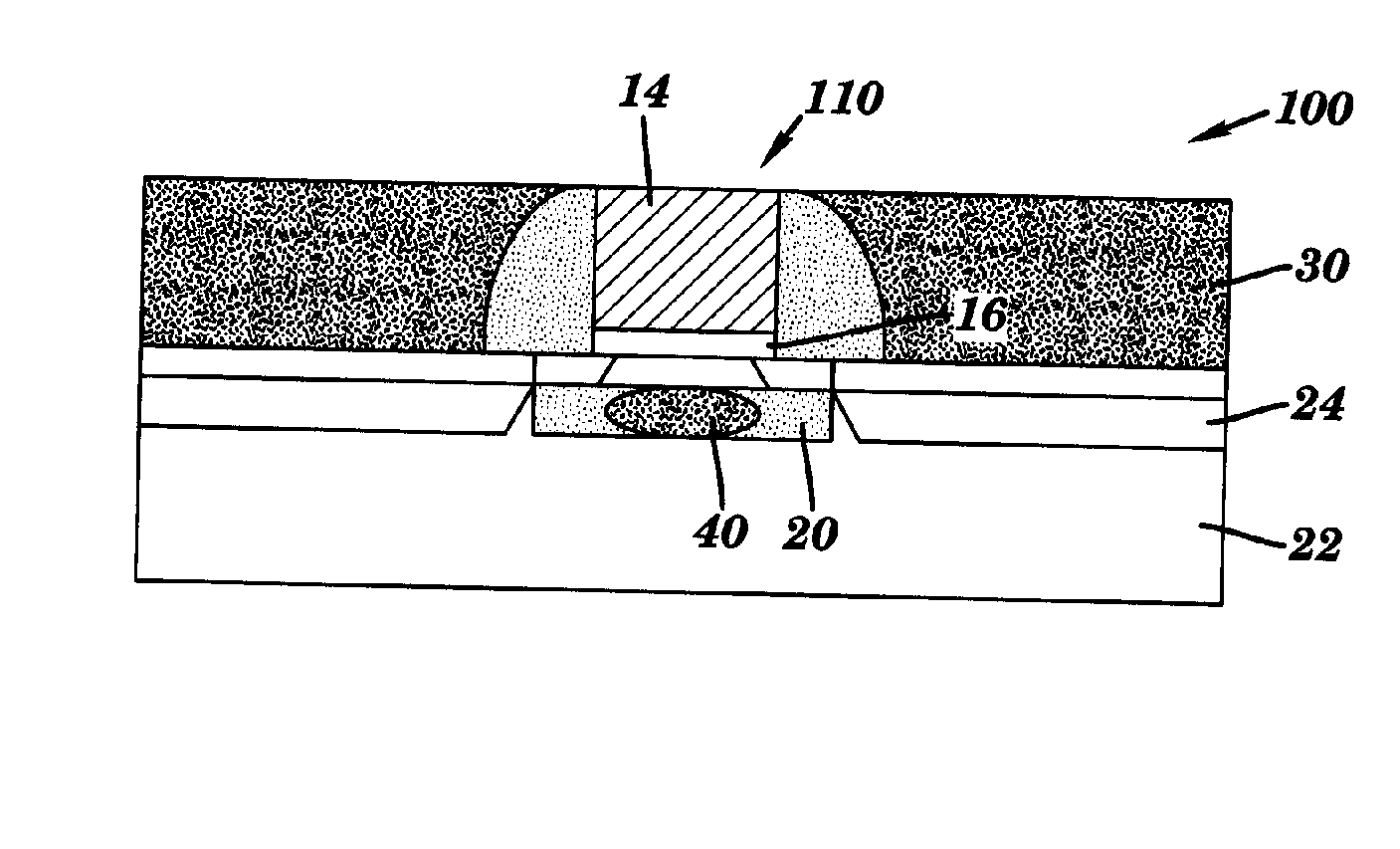
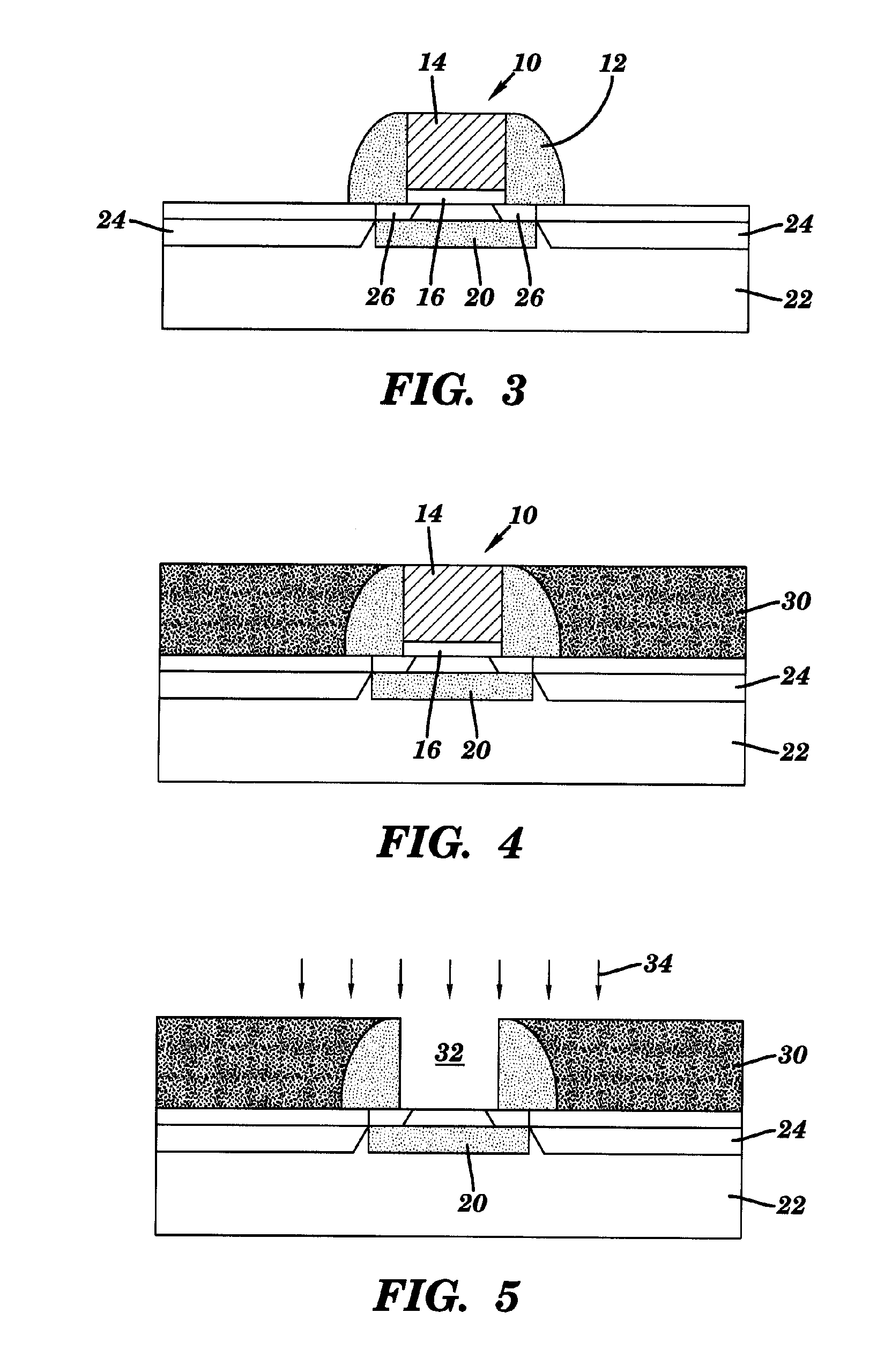
[0017] With reference to the accompanying drawings, FIG. 3 illustrates initial structure for a method of implementing a compensating dopant region according to the invention. As shown, a gate electrode 10 is provided including a spacer 12 surrounding a gate material area 14 and a gate dielectric 16. Gate electrode 10 is positioned over a well 20 in a substrate 22. Also shown are source-drain regions 24, and base extensions 26. In one embodiment, well 20 includes a super-steep retrograde well, as defined above. The type and amount of dopant in well 20 will vary depending on the type of device desired. For example, for an nFET, dopant would be p-type in well 20. In one embodiment, a super-steep retrograde well 20 has a dopant concentration greater than 5.0e18 / cm3, although this is not necessary.

[0018] As shown in FIG. 4, a next step includes forming a planar dielectric layer 30 about gate electrode 10. Planar dielectric layer 30 may be formed by deposition of, for example, silicon di...


PUM


Abstract

Methods and resulting structure of implementing a compensating implant that creates more compensation doping as the gate length is increased are disclosed. In particular, the invention performs an angled compensation implant through a gate opening during the damascene process such that the compensating dopant concentration increases as the gate length increases. In this fashion, the threshold voltage of a longer device is reduced much more than the threshold voltage of a shorter device, thereby reducing the threshold voltage of the longer device to acceptable levels without affecting the threshold voltage of the shorter device. The invention is especially advantageous relative to super-steep retrograde wells.

Description

BACKGROUND OF THE INVENTION [0001] 1. Technical Field [0002] The present invention relates generally to semiconductor device fabrication, and more particularly, to methods and resulting semiconductor device structure of implementing a channel compensating dopant region that creates more compensation doping as the gate length increases. [0003] 2. Related Art [0004] Reduction of threshold voltage is a continuing concern in semiconductor device structures. One particular structure in which threshold voltages are considered too high for long gate devices are super-steep retrograde well (SSRW) transistor devices. The term “retrograde well” indicates that the well is formed using an approach in which the highest concentration of dopant (implanted) in the well is located at a certain distance from the surface, which makes the device less susceptible to punch-through. The term “super-steep” indicates that the transition from the lower concentration of dopant to the higher concentration is f...

Claims


Application Information

Patent Timeline
Patent Type & Authority Applications(United States)
IPC IPC(8): H01L29/76H01L21/336
CPCH01L21/26586H01L21/268H01L29/66537H01L29/66545
Inventor DOKUMACI, OMER H.
Owner IBM CORP
Why Eureka
Try Eureka