
Elevated channel flash device and manufacturing method thereof

a flash device and elevated channel technology, applied in the direction of semiconductor devices, electrical apparatus, transistors, etc., can solve the problems of low operation speed, reliability issues, narrow operation voltage range (or cell window) of memory cells, etc., and achieve the effect of increasing the effective floating gate length

Inactive Publication Date: 2009-04-09
NAN YA TECH
View PDF2 Cites 6 Cited by
  • Summary
  • Abstract
  • Description
  • Claims
  • Application Information

AI Technical Summary

Benefits of technology

[0008]Accordingly, the present invention is directed to a FLASH device having an elevated channel, which increases an effective floating gate length without impacting cell density.
[0009]The present invention is also directed to a manufacturing method of a FLASH device, which increases an effective floating gate length without impacting cell density, and improves an operating voltage range (or cell window) of cells.
[0010]The present invention is further directed to a manufacturing method of a FLASH device, which increases an effective floating gate length, improves an operating voltage range of cells, and improves a coupling ratio.
[0029]Because the control gate of the FLASH device of the present invention is disposed on a protrusive portion, an elevated channel can be formed. Meanwhile, the floating gates are respectively disposed on two sides of the protrusive portion, and cover a portion of the top surface of the protrusive portion, so the effective floating gate length can be increased without impacting the cell density. Moreover, the operating voltage range of the cells can be improved and the coupling ratio can be increased according to the method of the present invention.

Problems solved by technology

However, the channel length of the FinFET-like FLASH is small due to the small device size and the structure, so the operating voltage range (or cell window) of the memory cells becomes very narrow.
Therefore, the operating voltage range of the cells must be expanded by increasing the programming voltage or pulse width, which, however, will lead to the reliability issue and low operation speed.
In addition, the cell density will be impacted if the operating voltage range of the cells is expanded by increasing the channel length.

Method used


Image

  • Elevated channel flash device and manufacturing method thereof
  • Elevated channel flash device and manufacturing method thereof
  • Elevated channel flash device and manufacturing method thereof

Examples


first embodiment

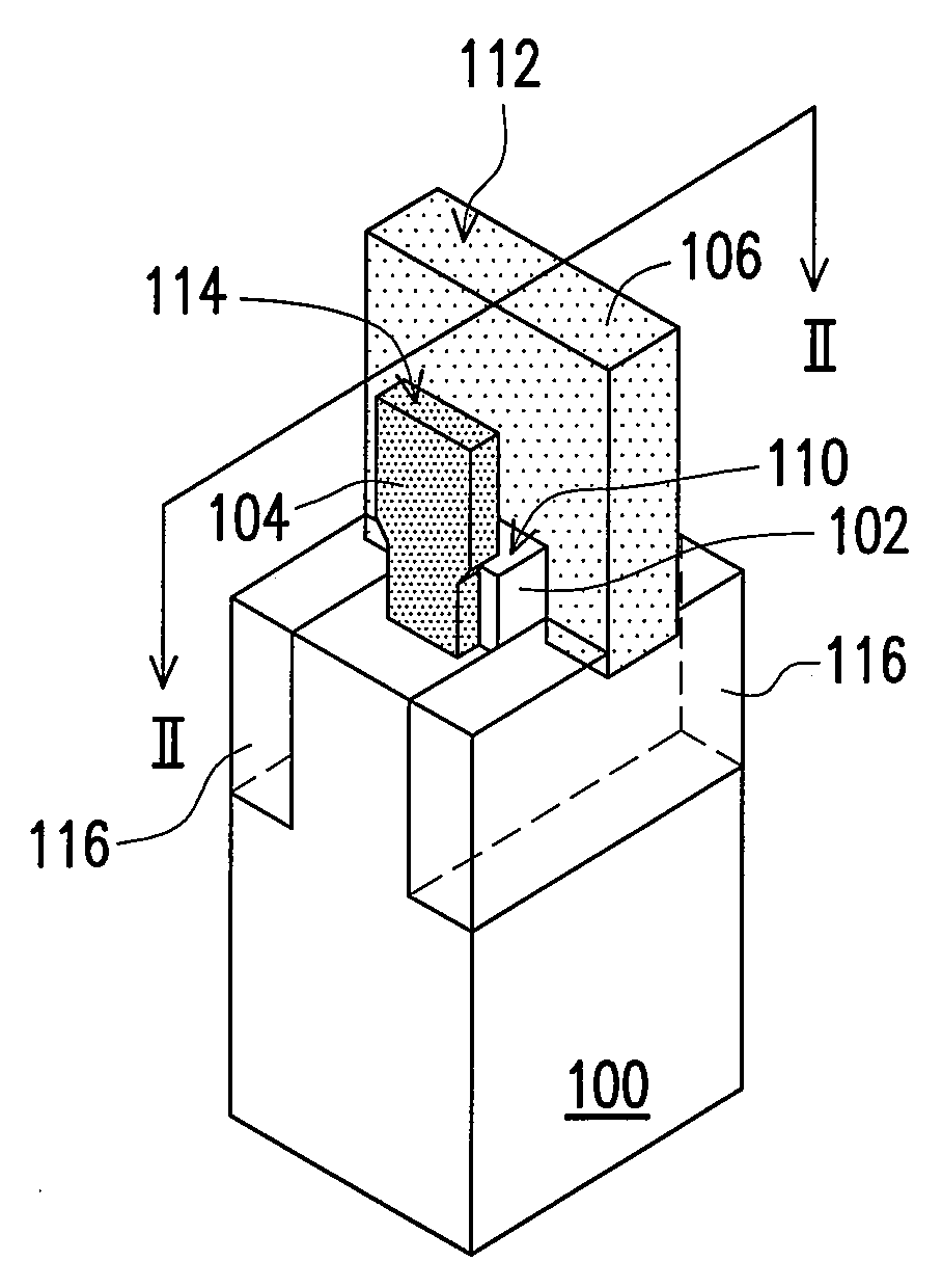
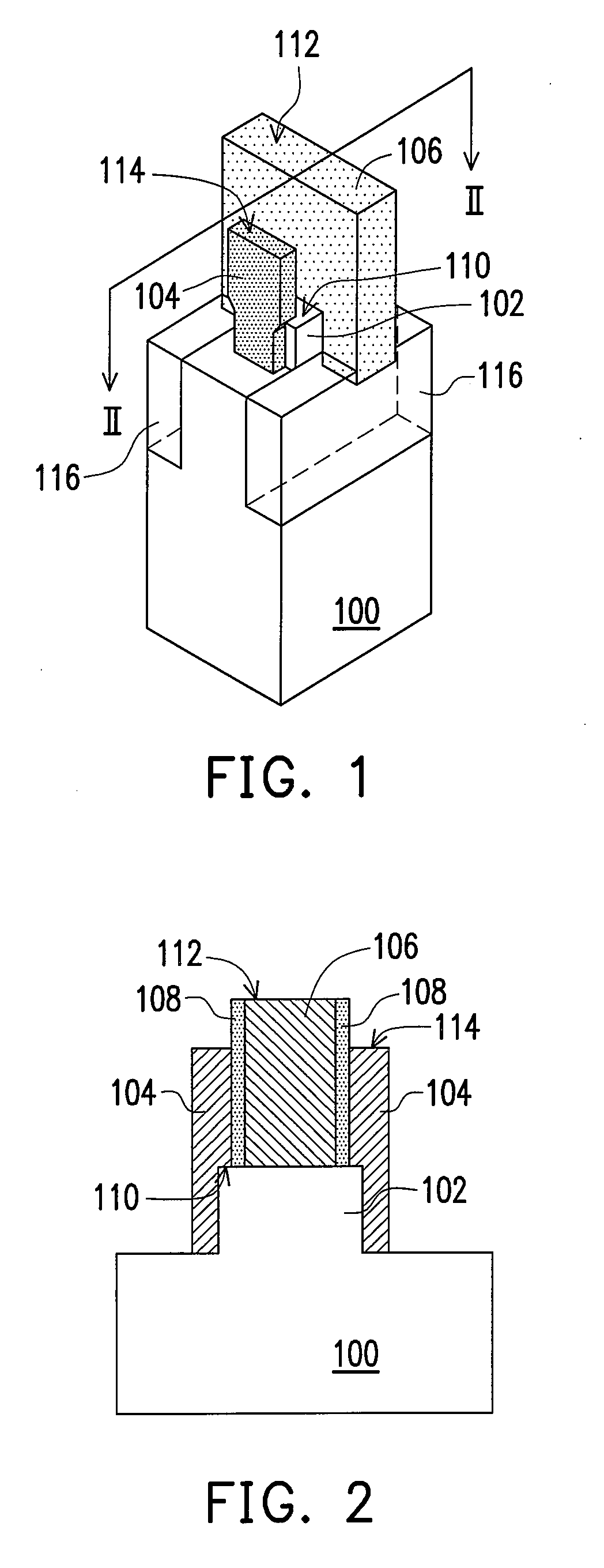
[0040]FIG. 1 is a perspective structural view of a FLASH device according to the present invention, in which some components are not shown for clarity. FIG. 2 is a cross-sectional view taken along line segment II-II in FIG. 1.

[0041]Referring to FIGS. 1 and 2, the FLASH device of the first embodiment includes a substrate 100 having a protrusion with a protrusive portion 102, two floating gates 104, a control gate 106, and a dielectric layer 108. The floating gates 104 are respectively disposed on two sides of the protrusive portion 102. A portion of a top surface 110 of the protrusive portion 102 is covered by the floating gates 104. The control gate 106 is disposed on top of the protrusive portion 102 and sandwiched between the floating gates 104. The dielectric layer 108 is disposed between each of the floating gates 104 and the control gate 106. In order to show the relative position of the control gate 106 and the floating gates104 clearly, the dielectric layer 108 is not shown i...

second embodiment

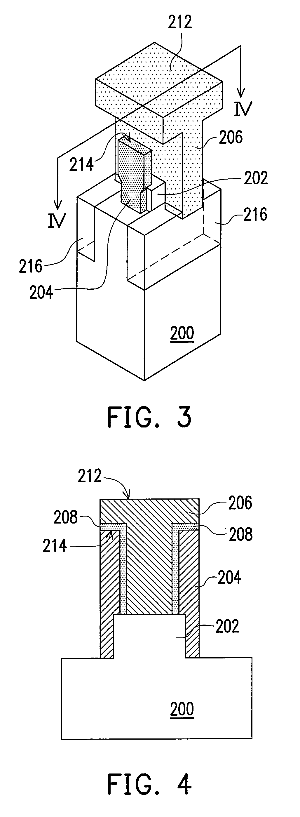
[0044]FIG. 3 is a perspective structural view of a FLASH device according to the present invention, in which some components are not shown. FIG. 4 is a cross-sectional view taken along line segment IV-IV in FIG. 3.

[0045]Referring to FIGS. 3 and 4, the FLASH device of the second embodiment includes a substrate 200 having a protrusive portion 202, two floating gates 204, a control gate 206, and a dielectric layer 208. The difference between the first and the second embodiments lies in the shape of the control gate 206. Here, the top surface of the control gate 206 laterally extends in two opposite directions to cover the top ends 214 top ends 214 of the two floating gates 204. Moreover, in order to show the relative position of the control gate 206 and the floating gates 204 clearly, the dielectric layer 208 is not shown in FIG. 3. In addition, FIG. 3 also includes isolation structures 216 and a protrusion formed on the substrate 200 and sandwiched between two of the isolation structu...

third embodiment

[0047]FIGS. 5A-5M are perspective views of the process to manufacture a FLASH device according to the present invention.

[0048]Referring to FIG. 5A, a substrate 500 is provided. The substrate 500 has a plurality of parallel isolation structures 502 such as STI structures.

[0049]Then, referring to FIG. 5B, a protrusive portion 504 is formed on the substrate 500 between two of the isolation structures 502. The method of forming the protrusive portion 504 is, for example, partially removing the substrate 500 between the isolation structures 502 as shown in this figure, or growing the protrusive portion on the substrate 500 by means of an epitaxy process.

[0050]Next, referring to FIG. 5C, a first conductive layer 506 is formed on the substrate 500 to cover the protrusive portion (not shown) and the isolation structures 502.

[0051]Then, referring to FIG. 5D, the first conductive layer above the isolation structures 502 (see 506 of FIG. 5C) is removed, so as to form a first strip of conductor...


PUM


Abstract

A FLASH device including a substrate having a protrusive portion integrally formed thereon, two floating gates, a control gate and a dielectric layer is provided. The two floating gates are disposed on two sides of the protrusive portion and respectively covering a portion of the protrusive portion. The control gate is disposed on top of the protrusive portion and sandwiched between the two floating gates. The dielectric layer is disposed between each of the two floating gates and the control gate. Because the control gate of the FLASH device is disposed on the protrusive portion, an elevated channel can be formed. Moreover, because of the position of the two floating gates, an effective floating gate (FG) length can be increased without impacting the cell density.

Description

CROSS-REFERENCE TO RELATED APPLICATION[0001]This application claims the priority benefit of Taiwan application serial no. 96137072, filed on Oct. 3, 2007. The entirety the above-mentioned patent application is hereby incorporated by reference herein and made a part of specification.BACKGROUND OF THE INVENTION[0002]1. Field of the Invention[0003]The present invention relates to a FLASH device technology. More particularly, the present invention relates to a FLASH device having an elevated channel and a manufacturing method thereof.[0004]2. Description of Related Art[0005]In various kinds of non-volatile memories, an electrically erasable programmable read-only memory (EEPROM), capable of saving programmed information without being limited by the ON / OFF of the power supply, has been widely used by personal computers and electronic devices. A non-volatile memory called “flash memory” has become one of the important memory elements on the market, due to the mature technology and low cos...

Claims


Application Information

Patent Timeline
Patent Type & Authority Applications(United States)
IPC IPC(8): H01L21/336H01L29/788
CPCH01L21/28273H01L29/7887H01L29/7851H01L29/66825H01L29/40114
Inventor WANG, JER-CHYICHANG, MING-CHENGCHANG, YI-FENGLIAO, WEI-MINGHUANG, CHIEN-CHANG
Owner NAN YA TECH
Learn More