
Semiconductor device and method of manufacturing the same

a technology of semiconductors and gate electrodes, applied in the direction of semiconductor devices, basic electric elements, electrical equipment, etc., can solve the problems of difficult to conduct patterning by dry etching, and achieve the effect of reducing the aspect ratio, preventing the increase of the aspect ratio of the gate electrode, and facilitating the patterning of the gate electrod

Inactive Publication Date: 2007-08-30
ELPIDA MEMORY INC
View PDF4 Cites 4 Cited by
  • Summary
  • Abstract
  • Description
  • Claims
  • Application Information

AI Technical Summary

Benefits of technology

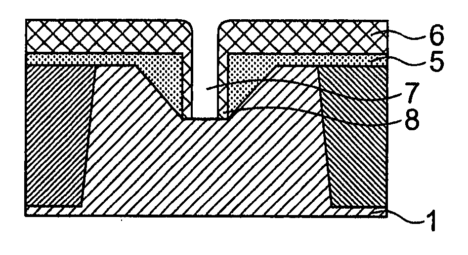
[0019] In order to produce a MOS transistor having a gate electrode on a slope according to the present invention, patterning is first conducted for a lower-layer gate electrode film near a lower end of the slope. Further, a space between the lower layers is filled with a filler so that the filler has the same height as a primary surface of a substrate. After an upper-layer gate electrode film is deposited, patterning is conducted on the gate electrode films. Since the space between the gate electrodes has the same height as the primary surface of the substrate, a contact hole can be opened with a reduced aspect ratio.

Problems solved by technology

Therefore, it problematically becomes difficult to conduct patterning by dry etching.

Method used


Image

  • Semiconductor device and method of manufacturing the same
  • Semiconductor device and method of manufacturing the same
  • Semiconductor device and method of manufacturing the same

Examples


Embodiment Construction

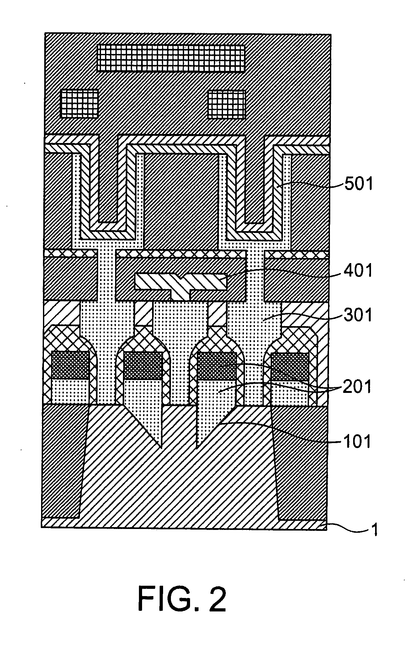
[0027] An embodiment of the present invention will be described below with reference to FIGS. 2 to 5D.

[0028]FIG. 2 is a cross-sectional view showing a memory cell portion of a dynamic random access memory (DRAM) according to an embodiment of the present invention. FIG. 2 shows memory cells of 2 bits, which are connected to a common bit line. As shown in FIG. 2, slopes 101 are formed in an active region of a silicon substrate 1. Gate electrodes 201 of MOS transistors are provided on the slopes 101 with a gate insulating film formed between the slopes 101 and the gate electrodes 201. The gate insulating film is so thin that it is not illustrated in FIG. 2. With the gate electrodes 201 having the above arrangement, channel portions are formed on the slopes. Accordingly, it is possible to make a channel length of the transistor larger than the width of the gate electrode 201. Consequently, even if the device is reduced in size, it is possible to prevent degradation in characteristics o...


PUM


Abstract

In order to produce a MOS transistor having a gate electrode on a slope, patterning is first performed for a lower-layer gate electrode film near a lower end of the slope. A space between the lower-layer gate electrode films is filled with a filler so that the filler has the same height as a primary surface of a substrate. After an upper-layer gate electrode film is deposited, patterning is performed for the gate electrode films.

Description

[0001] This application claims priority to prior Japanese patent application JP2006-36791, the disclosure of which is incorporated herein by reference. BACKGROUND OF THE INVENTION [0002] 1. Field of the Invention [0003] The present invention relates to a semiconductor device, and more particularly to a semiconductor device having a MOS transistor formed on a slope of a semiconductor substrate. The present invention also relates to a method of manufacturing such a semiconductor device. [0004] 2. Description of the Related Art [0005] Recently, semiconductor devices have made remarkable progress. For example, integration of semiconductor elements in a dynamic random access memory (DRAM) has more than doubled approximately every 12 months to 18 months. In order to achieve higher integration of semiconductor elements, Metal-Oxide-Semiconductor (MOS) transistors have been reduced in size. The reduction of the size may cause performance of a MOS transistor to be degraded by a short channel...

Claims


Application Information

Patent Timeline
Patent Type & Authority Applications(United States)
IPC IPC(8): H01L21/336H01L21/8242H01L21/3205
CPCH01L29/1037H01L27/10876H10B12/053
Inventor YOKOI, NAOKI
Owner ELPIDA MEMORY INC
Learn More