Methods for gate-length biasing using annotation data

a gate-length biasing and annotation data technology, applied in the field of digital integrated circuit optimization, can solve the problems of linear delay, exponential decrease in leakage power, and impairing time delay performance only linearly, so as to reduce leakage power and variability of chips, reduce the impact of existing design and/or manufacturing processes, and increase the design space

Inactive Publication Date: 2010-07-01
RPX CORP
View PDF41 Cites 22 Cited by
  • Summary
  • Abstract
  • Description
  • Claims
  • Application Information

AI Technical Summary

Benefits of technology

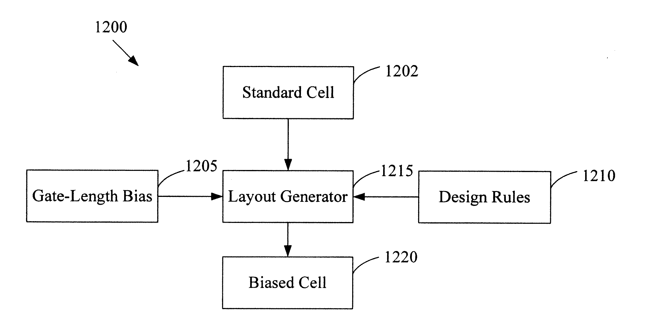
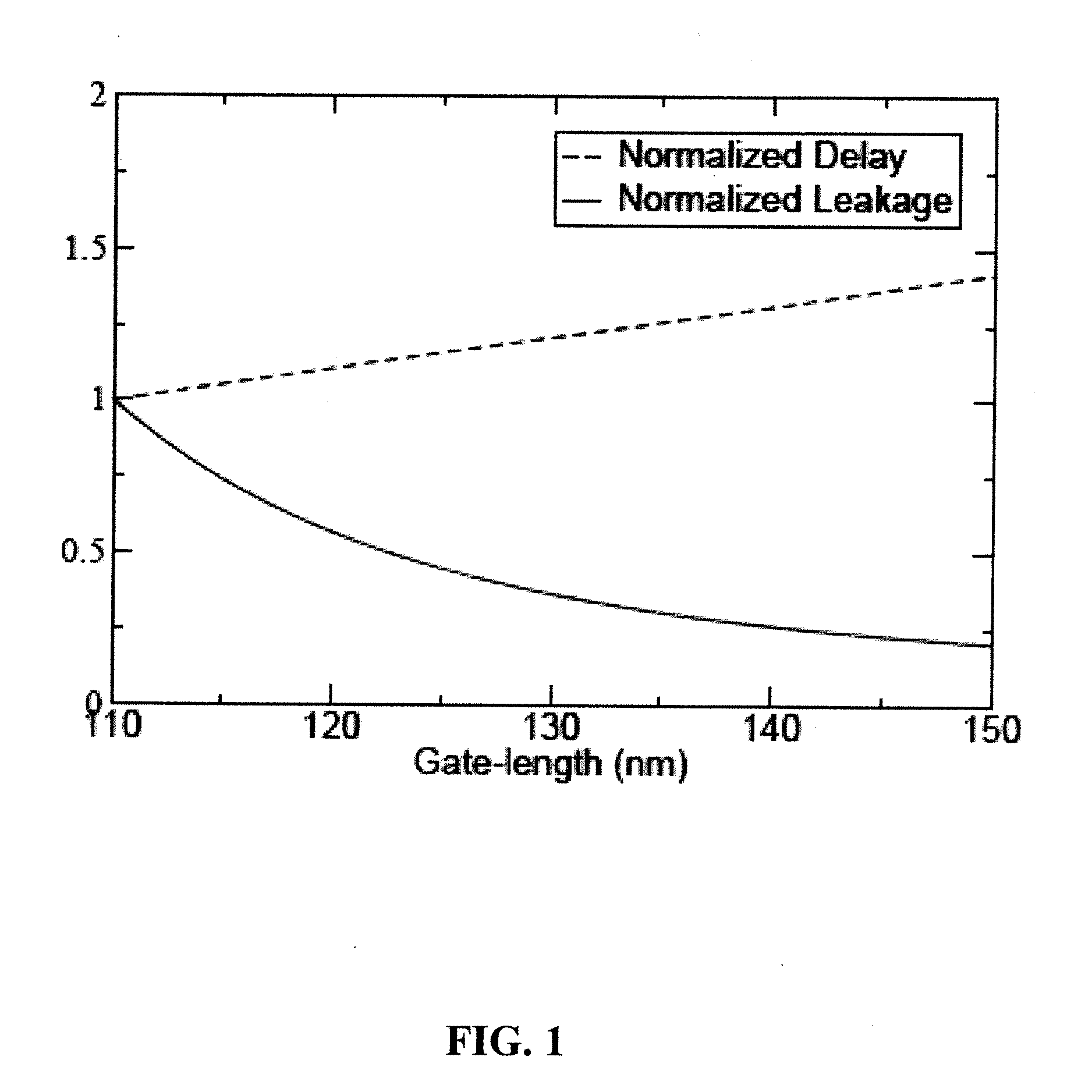
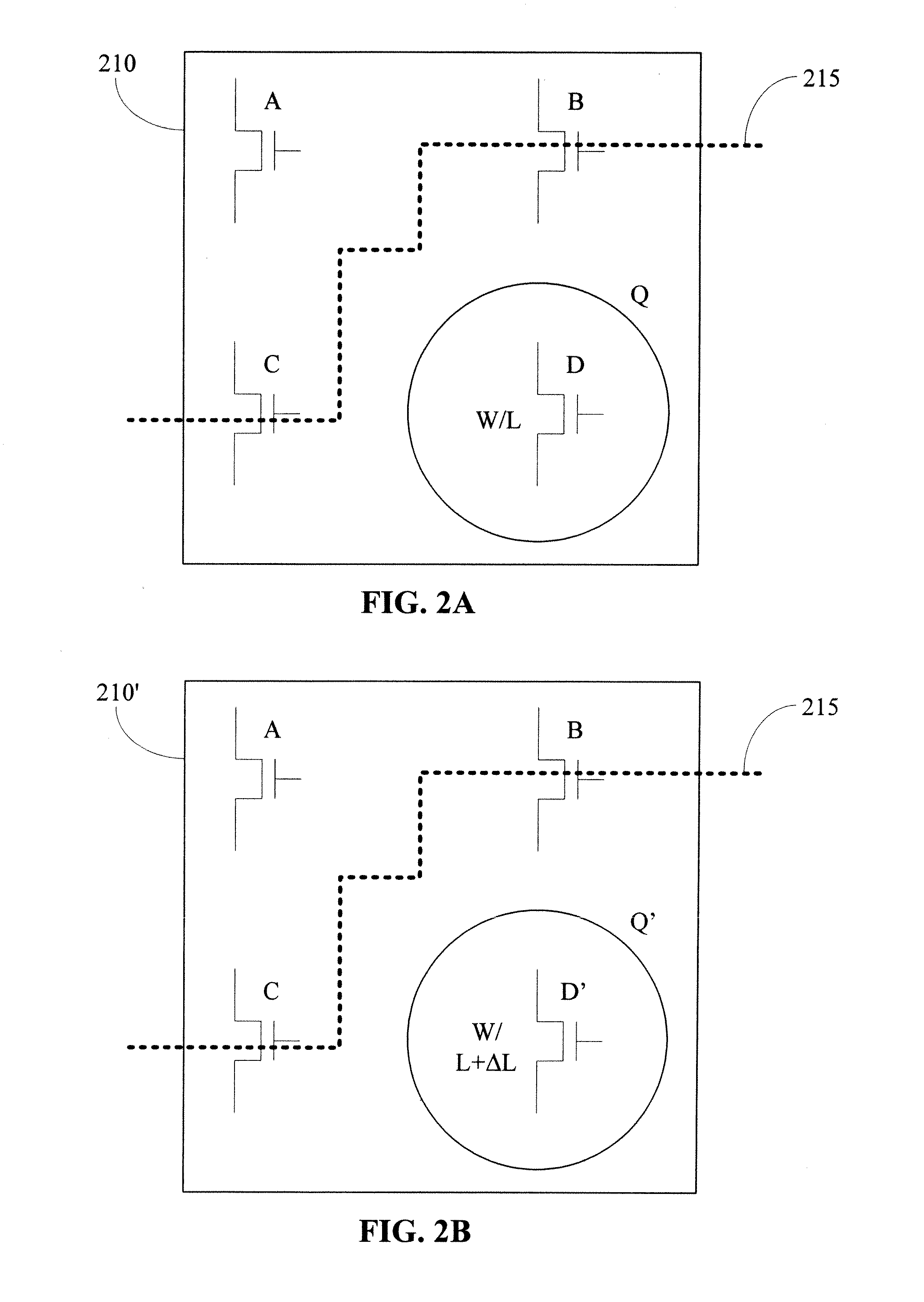
[0014]The present invention overcomes the limitations of the prior art by providing small biasing of device gate-lengths, preferably in a manner that has low impact on existing design and / or manufacturing processes. For example, biasing of device gate-lengths affords an additional design space to reduce chip leakage power and its variability. Typically, leakage power decreases exponentially, and delay increases linearly, with increasing gate-length. Thus, it is possible to increase gate-length only marginally to take advantage of the exponential leakage reduction, while impairing time delay performance only linearly. From a design flow standpoint, the use of only slight increases in gate-length can preserve pin- and layout-compatibility. Therefore, the technique can be applied, for example, as a post-layout enhancement step. Application of gate-length biasing, primarily to those devices that do not appear in critical paths, can achieve zero or negligible degradation in delay characteristics for the chip.
[0016]Small gate-length biasing can also be used for various other purposes. For example, it may be used to reduce various types of power consumption (e.g., total power, static power or dynamic power), preferably in a manner that has minimal or zero impact on timing delays. Decreasing gate-lengths of certain devices can reduce time delays or increase the operating frequency of the chip. Gate-length biasing may also be used to increase the on-chip signal integrity. As a final example, gate-length biasing may be used for manufacturability purposes: for example, to increase the reliability or manufacturability of the chip. The amount and sign of the biasing and the specific transistors to be biased will depend in part on the purpose of the biasing. Biasing can be positive (to longer gate-lengths) or negative (to shorter gate-lengths), depending on the application.
[0018]In another exemplary embodiment, the gate-length biasing methodology may be implemented using optical proximity correction to apply the small bias length to particular transistors in a nominal layout. The implementation may include one or more of, for example, shifting a required error tolerance, applying a starting edge offset, using a maximum error tolerance, accounting for iso-dense layout effects, or other techniques.

Problems solved by technology

Typically, leakage power decreases exponentially, and delay increases linearly, with increasing gate-length.
Thus, it is possible to increase gate-length only marginally to take advantage of the exponential leakage reduction, while impairing time delay performance only linearly.

Method used


Image

  • Methods for gate-length biasing using annotation data
  • Methods for gate-length biasing using annotation data
  • Methods for gate-length biasing using annotation data

Examples


experimental examples

[0079]A test flow for validation of the LGate biasing methodology was implemented in the context of leakage reduction. Seven test cases were chosen for investigation. Details of the test cases used in the experiments are given in Table 3. For each test case, Table 3 shows the source of the test case, the number of cells in the circuit, delay, leakage power, and dynamic power. Sequential test cases (e.g., those beginning with “s”) were handled by converting them to combinational circuits by treating all flip-flops as primary inputs and primary outputs. The test flow was designed to validate an LGate biasing methodology in which CLLB was performed first followed by TLLB to show further reductions in leakage. Thus, while library generation and design optimization are discussed primarily with respect to the CLLB method, the discussion applies as well to the TLLB method.

TABLE 3TestDelayDynamicCaseSource#Cells(ns)Leakage (mW)(mW)s9234ISCAS′898610.4370.70740.3907c5315ISCAS′8514420.5561.441...


PUM


Abstract

Methods for generating a biased layout for making an integrated circuit are disclosed. One such method includes obtaining a nominal layout defined by one or more cells, where each cell has one or more transistor gate features with a nominal gate length. Then, obtaining an annotated layout. The annotated layout contains information describing gate-length biasing of one or more of the transistor gate features in one or more cells of the nominal layout. A biased layout is produced by modifying the nominal layout using the information from the annotated layout. The biasing modifies a gate length of those transistor gate features identified by the information of the annotated layout.

Description

CLAIM OF PRIORITY TO RELATED APPLICATION[0001]This application is a continuation and claims priority under 35 U.S.C. §120, from pending U.S. patent application Ser. No. 12 / 212,353, filed on Sep. 17, 2008, which claims priority from U.S. patent application Ser. No. 11 / 145,025, filed on Jun. 3, 2005, now U.S. Pat. No. 7,441,211, which claimed priority from U.S. Provisional Patent Application No. 60 / 678,694, filed on May 6, 2005.Each of the above-identified applications are incorporated herein by reference.BACKGROUND OF THE INVENTION[0002]1. Field of the Invention[0003]This invention relates generally to optimization of digital integrated circuits, and more particularly, to small gate-length biasing of transistors to improve performance characteristics.[0004]2. Description of the Related Art[0005]Modern-day digital integrated circuits are complex devices that often must meet high performance standards. Due to their complexity, the design and simulation of integrated circuits is also a ...

Claims


Application Information

Patent Timeline
Patent Type & Authority Applications(United States)
IPC IPC(8): G06F17/50
CPCH01L27/0207H01L27/11807G06F30/36G06F30/39G06F30/398G06F2119/06G06F2119/12G06F30/373
Inventor GUPTA, PUNEETKAHNG, ANDREW B.
Owner RPX CORP
Why Eureka
Try Eureka