Optical module and method of manufacturing the same

a technology of optical modules and optical light guides, applied in the field of optical modules, can solve the problems of inability to improve the bonding strength and the uneven thickness of the resin applied to the circumference of the stem portion, and achieve the effect of reducing the deviation in optical alignmen

Active Publication Date: 2006-07-20
SUMITOMO ELECTRIC IND LTD
View PDF1 Cites 12 Cited by
  • Summary
  • Abstract
  • Description
  • Claims
  • Application Information

AI Technical Summary

Benefits of technology

[0007] An object of the present invention is to offer an optical module having a structure that can reduce the deviation in optical alignment at the time of the assembly work to a small magnitude. Another object is to offer a method of producing the foregoing optical module.

Problems solved by technology

Because the center of the external shape of the optically aligned housing is not coincident with that of the optical device, the thickness of the resin applied to the circumference of the stem portion is not uniform.
Therefore, the bonding strength cannot be improved notably by the application of the thermosetting resin.

Method used


Image

  • Optical module and method of manufacturing the same
  • Optical module and method of manufacturing the same
  • Optical module and method of manufacturing the same

Examples


first embodiment

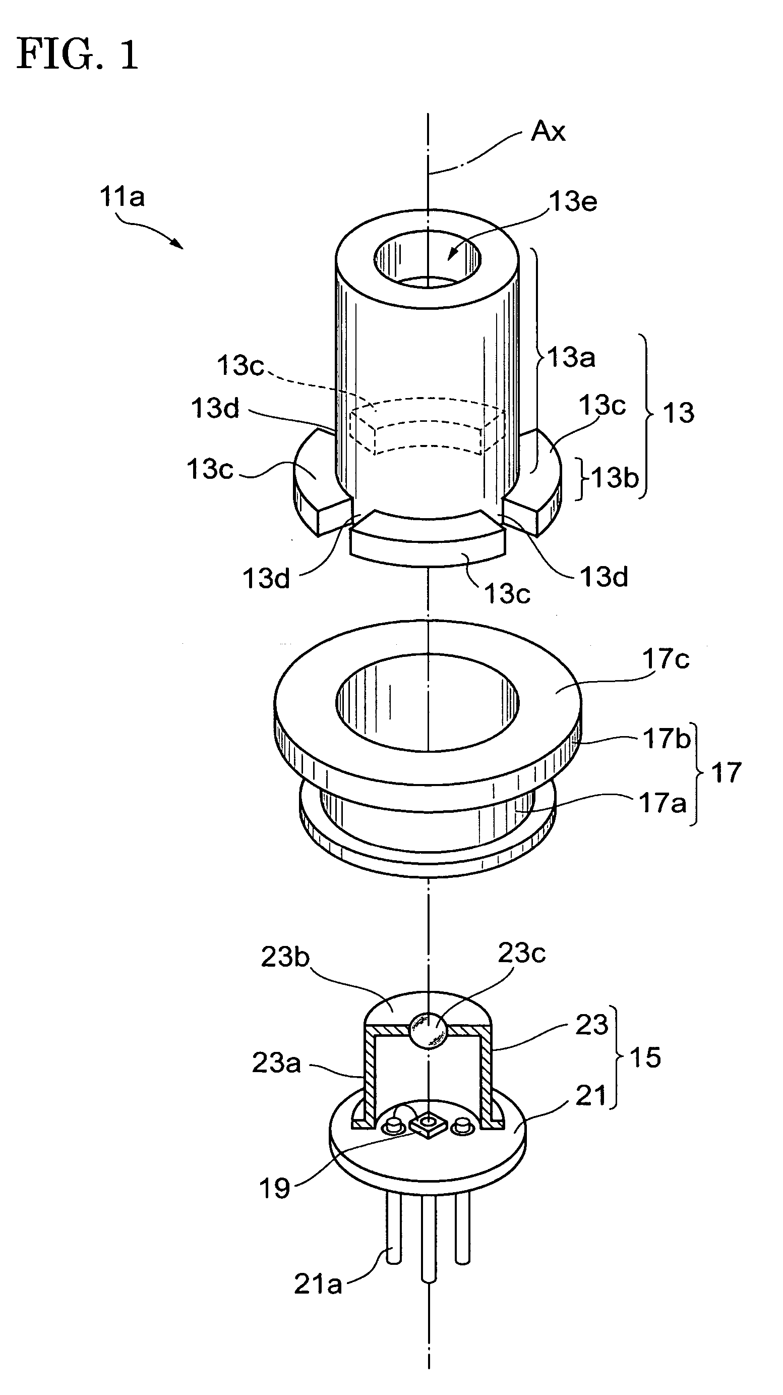
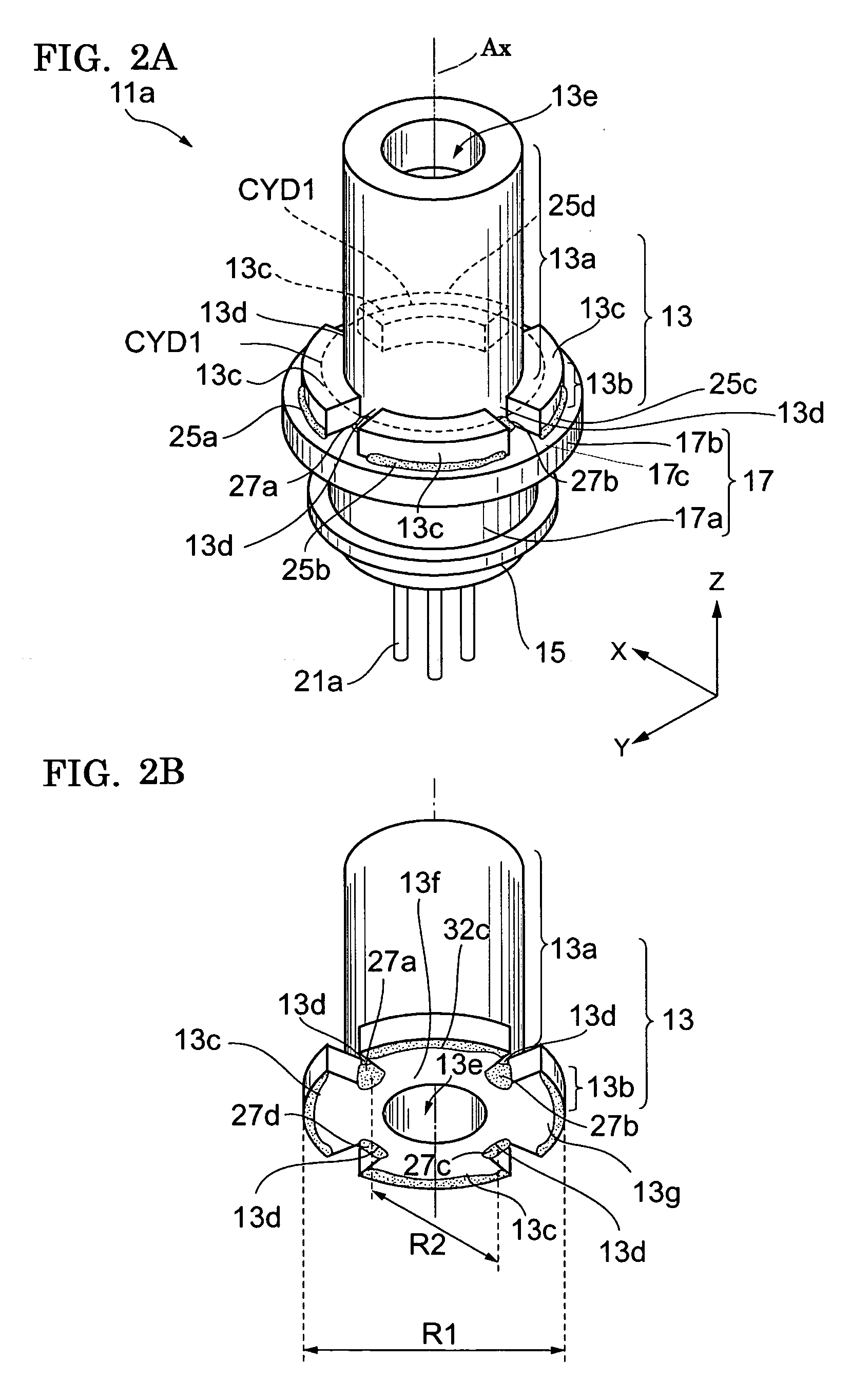
[0080]FIG. 1 is a diagram showing components that constitute an optical module in a first embodiment. FIG. 2A is a diagram showing an optical module in the first embodiment, and FIG. 2B is a diagram showing an optical-receptacle housing of the optical module. An optical module 11a comprises an optical-receptacle housing 13, an optical-communication subassembly 15, and a holder 17. The optical-receptacle housing 13 has a receptacle portion 13a, which extends along a predetermined axis, Ax, and a flange portion 13b provided at one end of the receptacle portion 13a. The axis Ax can be positioned at the center of the optical-receptacle housing. The optical-communication subassembly 15 has a stem 21, which mounts a semiconductor optical device 19, and a cap 23 covering the semiconductor optical device 19. The holder 17 has a side-wall portion 17a, which extends along the predetermined axis, and a mounting portion 17b provided at one end of the side-wall portion 17a to mount the optical-r...

second embodiment

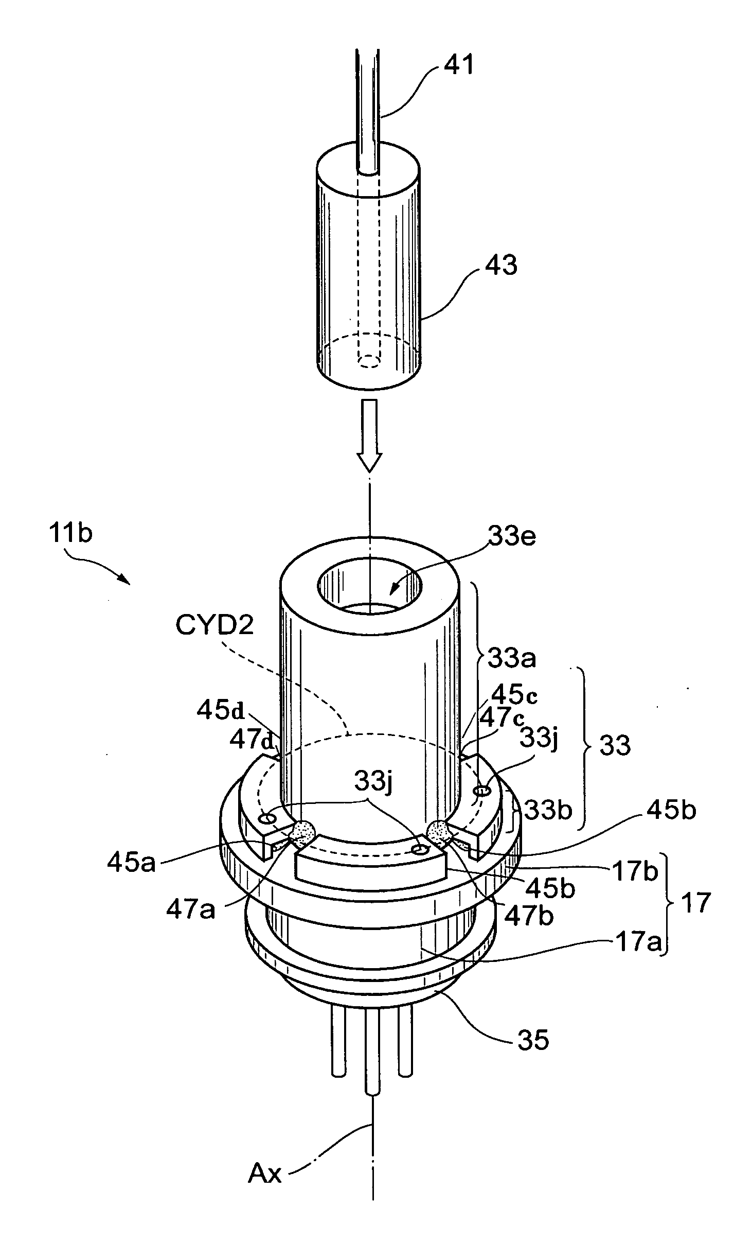
[0091]FIG. 3 is a diagram showing components that constitute an optical module in a second embodiment. FIG. 4 is a diagram showing an optical module in the second embodiment. An optical module 11b comprises an optical-receptacle housing 33, an optical-communication subassembly 35, and a holder 17. The optical-receptacle housing 33 has a receptacle portion 33a, which extends along a predetermined axis, Ax, and a flange portion 33b provided at one end of the receptacle portion 33a. The optical-communication subassembly 35 has a stem 31, which mounts a semiconductor optical device 39, and a cap 23 covering the semiconductor optical device 39. The holder 17 holds the optical-communication subassembly 35 and optically positions the optical-receptacle housing 33 and the optical-communication subassembly 35 with each other. In an example, the optical-receptacle housing 33 and the holder 17 are made of metal.

[0092] The flange portion 33b has a plurality of first portions 33c, which extend ...

third embodiment

[0100]FIG. 6 is a diagram for explaining an optical-module-producing method in a third embodiment. To produce an optical module, the optical-communication subassembly 15, the holder 17, and the optical-receptacle housing 13 are prepared. The optical-communication subassembly 15 is aligned with the holder 17. The optical-communication subassembly 15, the holder 17, and the optical-receptacle housing 13 are held by an assembly tool 51. The assembly tool 51 is used to optically align the optical-receptacle housing 13 with the optical-communication subassembly 15 by, for example, moving the optical-receptacle housing 13 in the X, Y, and Z directions. Lead terminals of the optical-communication subassembly 15 are connected to a measuring tool or power-supply device 55 to electrically connect the semiconductor optical device through connecting wires 53. A ferrule 57 is inserted into the optical-receptacle housing 13. An optical fiber 59 is attached to the ferrule 57. The optical fiber 59 ...


PUM


Abstract

An optical module 11a comprises an optical-receptacle housing 13, an optical-communication subassembly 15, and a holder 17. The flange portion 13b has a plurality of first portions 13c, which extend along a reference plane perpendicular to a predetermined axis, Ax, and a plurality of second portions 13d, each of which is positioned between the first portions 13c. The outer periphery of the first portions 13c is positioned at the outside of a reference cylinder whose center is coincident with the predetermined axis Ax. The outer periphery of the second portions 13d is positioned at the inside of the reference cylinder. The optical-receptacle housing 13 and the holder 17 are temporarily fixed to each other at the second portions 13d of the flange portion 13b through second bonding members 27a to 27d. The optical-receptacle housing 13 and the holder 17 are further fixed with increased strength to each other at the first portions 13c of the flange portion 13b through first bonding members 25a to 25d. As a result, the deviation in optical alignment can be decreased to a small magnitude.

Description

BACKGROUND OF THE INVENTION [0001] 1. Field of the Invention [0002] The present invention relates to an optical module and a method of producing the optical module. [0003] 2. Description of the Background Art [0004] The published Japanese patent application Tokukai 2002-90587 describes a method of producing an optical module. According to this method of producing an optical module, ultraviolet / heat-curable resin is applied in the shape of the circumference of a circle onto a surface for bonding with a stem portion at the end portion of a housing that mounts an optical semiconductor device. In a temporary fixing step, after a lens and an optical semiconductor device are optically aligned and bonded with each other, ultraviolet rays are radiated from the outside of the stem portion to ultraviolet-cure the ultraviolet / heat-curable resin. In a complementary curing step, the ultraviolet / heat-curable resin is heated to heat-cure the ultraviolet-unirradiated portion. In a bonding-reinforci...

Claims


Application Information

Patent Timeline
Patent Type & Authority Applications(United States)
IPC IPC(8): G02B6/36
CPCG02B6/4225G02B6/4226G02B6/4228G02B6/4292
Inventor NISHIE, MITSUAKINAKANISHI, HIROMIHIRAYAMA, KENJI
Owner SUMITOMO ELECTRIC IND LTD
Why Eureka
Try Eureka