

Printing of organic electronic devices
a printing and electronic device technology, applied in the direction of solid-state devices, transportation and packaging, coatings, etc., can solve the problems of affecting the useful part of the device, electrical characteristics not very constant, etc., to reduce the evaporation rate of ink, increase the drying time of solution, and uniform and flatter profile
- Summary
- Abstract
- Description
- Claims
- Application Information
AI Technical Summary
Benefits of technology
Problems solved by technology
Method used
Image

Examples
Embodiment Construction
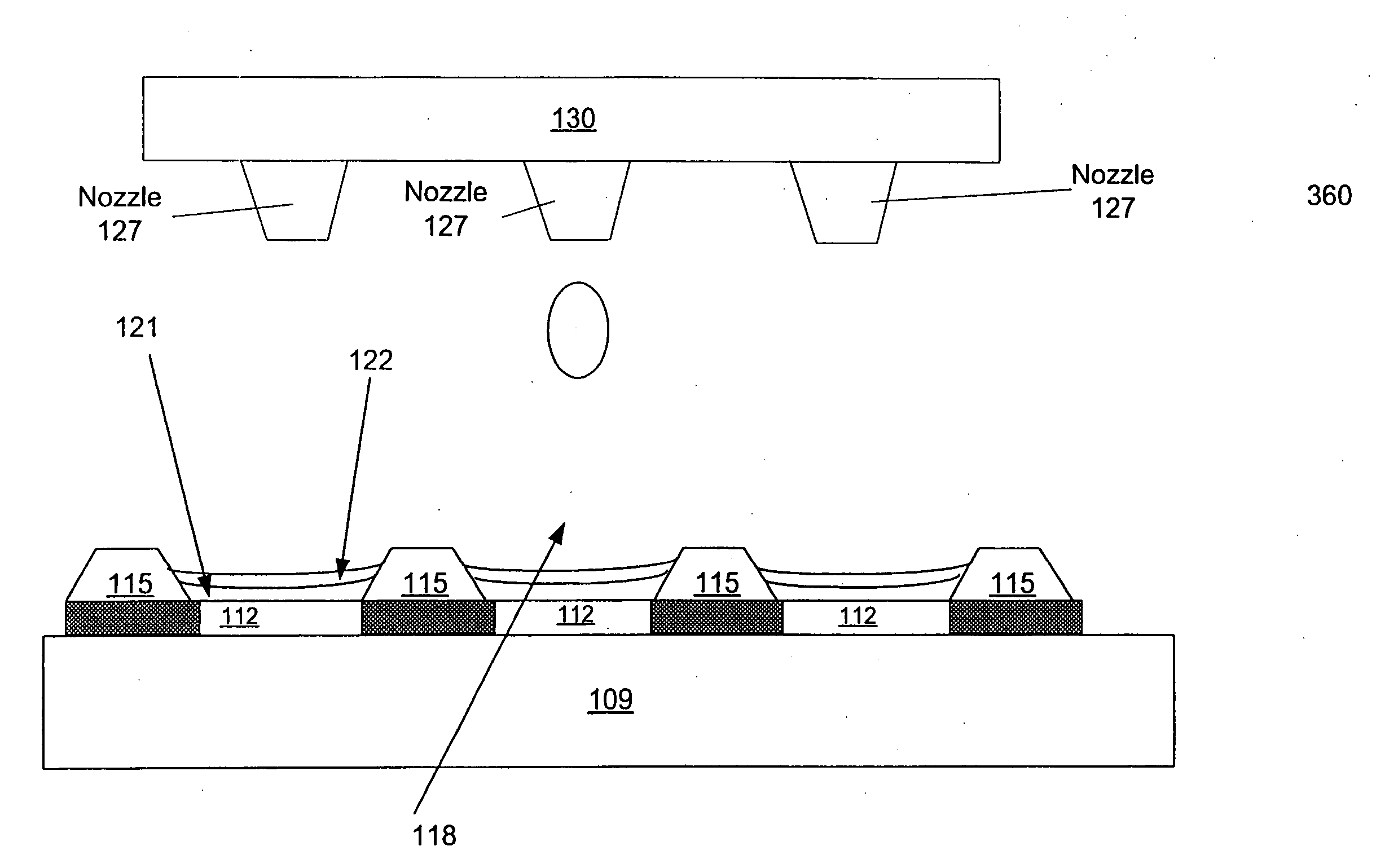
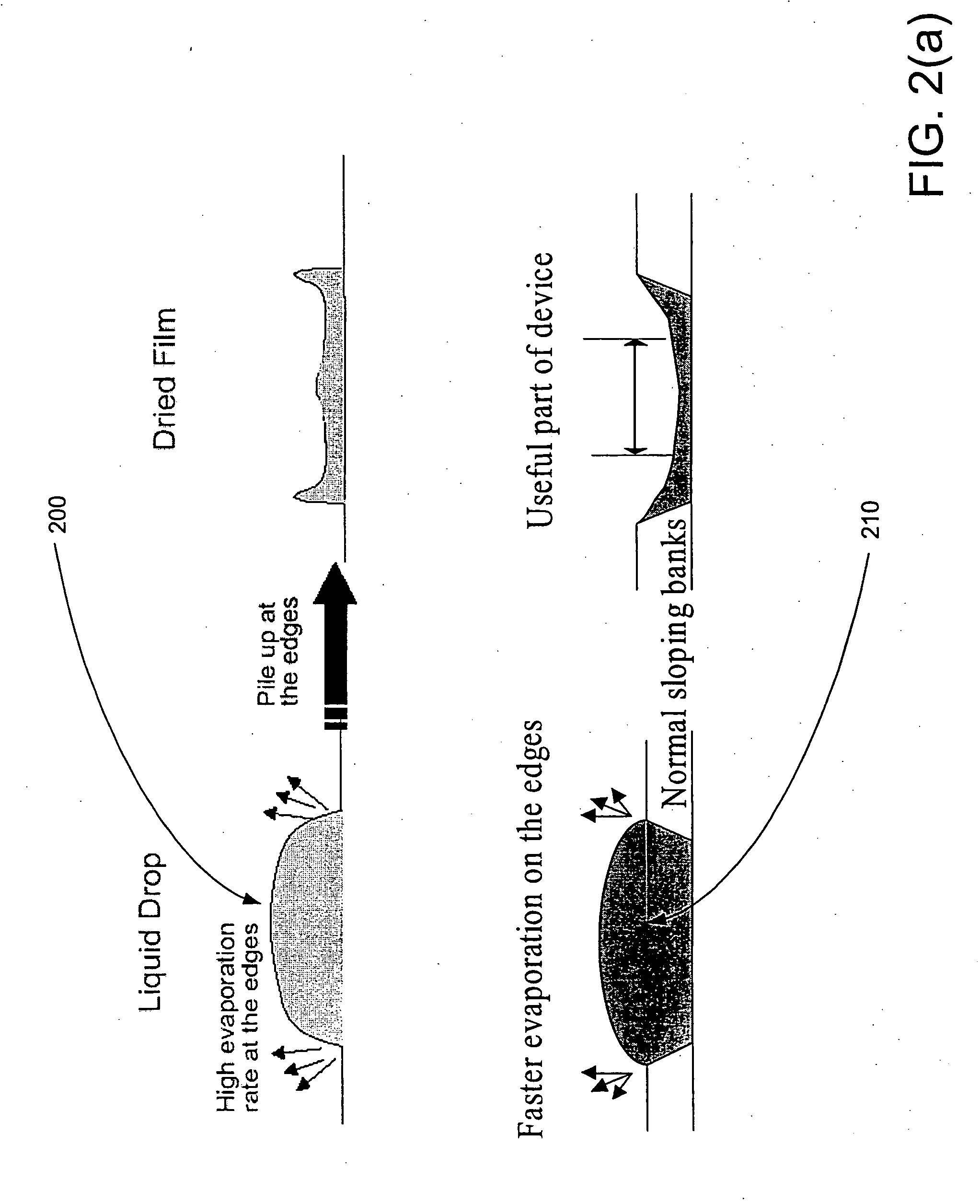
[0022] In accordance with the invention, the composition of an organic (e.g. conducting polymer) solution is reformulated and the device, upon which the reformulated solution is to be deposited, is treated prior to deposition. This reformulation and device treatment induces a more uniform and flatter profile when the reformulated organic solution is allowed to dry into a film on a surface of the treated device.
[0023] In the case of an OLED, the organic solution is a conducting polymer solution. The reformulation of conducting polymer solution involves mixing a base conducting polymer solution with humectants and water. The humectants help to increase the drying time of the solution by decreasing the evaporation rate of the ink while the water serves to lower the solids content of the reformulated conducting polymer solution. In addition, the OLED upon which the reformulated conducting polymer solution is to be deposited is treated with a fluorinating plasma. This treatment modifies...
PUM
| Property | Measurement | Unit |
|---|---|---|
| work function | aaaaa | aaaaa |
| thickness | aaaaa | aaaaa |
| thickness | aaaaa | aaaaa |
Abstract
Description
Claims
Application Information