Structure and method to enhance stress in a channel of CMOS devices using a thin gate

a thin gate and channel technology, applied in the field of cmos devices, can solve the problems of difficult to apply a large stress in the channel with known methods, limited methods of producing stressed films, and thin gate cmos devices that cannot support relatively large stresses in the channel region

Inactive Publication Date: 2006-07-20
IBM CORP
View PDF99 Cites 58 Cited by
  • Summary
  • Abstract
  • Description
  • Claims
  • Application Information

AI Technical Summary

Benefits of technology

[0012] In another aspect of the invention, a CMOS device includes a gate structure on a substrate, and a first stressed film arranged on the subs

Problems solved by technology

It should be noted that such methods of producing a stressed film are limited to producing a stress film with an internal stress on the order of a couple of GigaPascal (GPa).
Thus, thin gate CMOS devices typically can not support relatively large stresses in the channel region.
Although electron and hole mobilit

Method used


Image

  • Structure and method to enhance stress in a channel of CMOS devices using a thin gate
  • Structure and method to enhance stress in a channel of CMOS devices using a thin gate
  • Structure and method to enhance stress in a channel of CMOS devices using a thin gate

Examples


Embodiment Construction

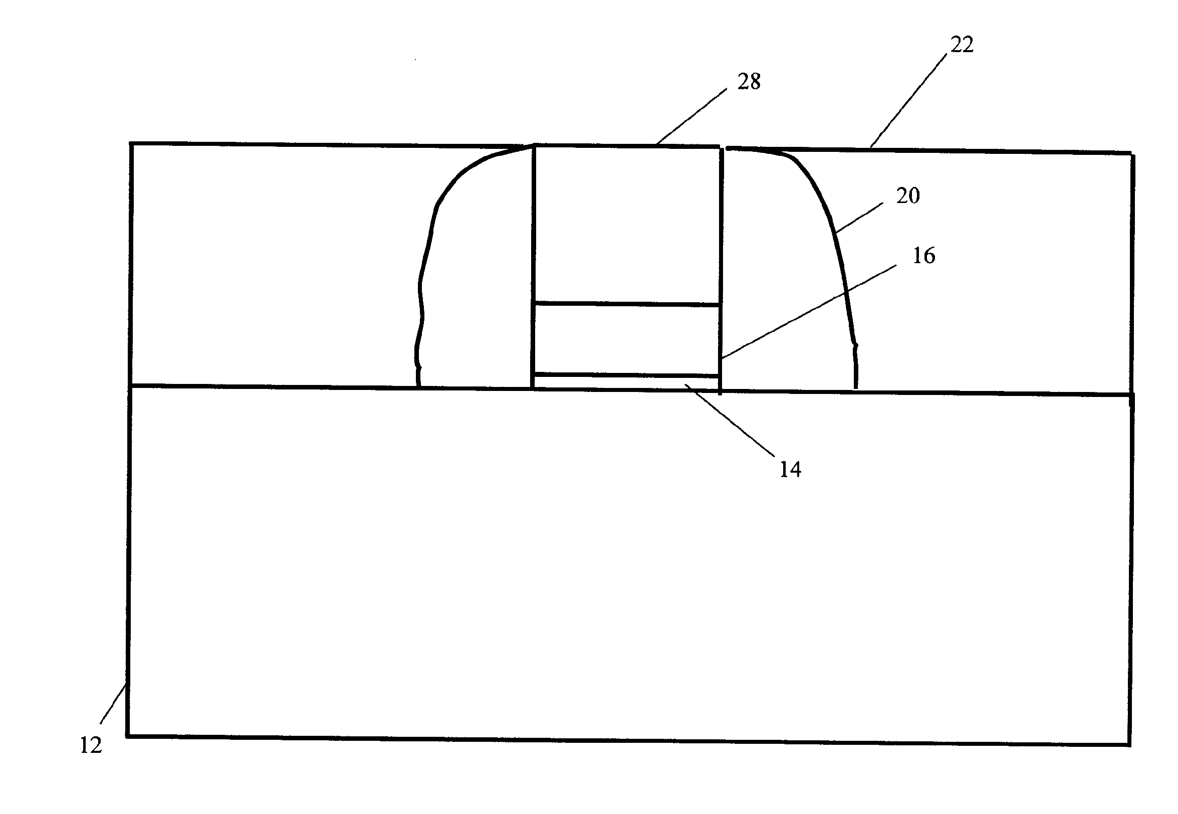
[0016] The invention is directed, for example, to enhancing stress in the channel of a CMOS device using a thin gate by forming a taller or 2-layer gate stack or structure, and selectively removing a top part of the gate structure to achieve a thin gate after deposition of a stressed film. Accordingly, a higher stress can be induced in the CMOS channel from the stressed film than would be with a shorter or single gate stock. Additionally, the top parts of CMOS devices so formed can be selectively etched to meet various design criteria. For example, an n-FET gate can be selectively etched to enhance the n-FET performance without degrading p-FET performance if one type of tensile film is deposited on top of the n-FET and p-FET devices. If a dual stressed film with different types of stress, such as for example, a tensile film on an n-FET and a compressive film on a p-FET is used, both n-FET and p-FET gates can be removed to enhance the stress in the respective channel. Thus, the metho...


PUM


Abstract

A method and structure for producing CMOS devices having thin gates with enhanced stress in a stressed channel is provided. The method allows for producing a CMOS device with a relatively thin gate to provide improved gate response characteristics. Additionally, the structure includes a first stressed film having a raised portion which extends above a top surface of the thin gate. By providing a raised portion of the first stressed film extending about a top surface of the gate, a relatively thick layer of the first stressed film as compared to the thickness of the thin gate is included in the CMOS device and thus allows for higher stress levels in the stressed channel. Additionally, a second stressed film having a stress direction opposite to that of the first stressed film may be included above the thin gate to further enhance the stress in the stressed channel of the CMOS device.

Description

BACKGROUND OF THE INVENTION [0001] The invention relates to CMOS devices, and more particularly to CMOS devices with stressed channels and thin gates. [0002] Metal-oxide semiconductor transistors generally include a substrate made of a semiconductor material, such as silicon. The transistors typically include a source region, a channel region and a drain region within the substrate. The channel region is located between the source and the drain regions. A gate stack, which usually includes a conductive material, a gate oxide layer and sidewall spacers, is generally provided above the channel region. More particularly, the gate oxide layer is typically provided on the substrate over the channel region, while the gate conductor is usually provided above the gate oxide layer. The sidewall spacers help protect the sidewalls of the gate conductor. [0003] It is known that the amount of current flowing through a channel which has a given electric field across it is generally directly propo...

Claims


Application Information

Patent Timeline
IPC IPC(8): H01L21/8228
CPCH01L21/2807H01L21/823807H01L21/823828H01L29/66545H01L29/78H01L29/7843
Inventor ZHU, HUILONGYANG, HAINING S.GLUSCHENKOV, OLEGCHIDAMBARRAO, DURESETILUO, ZHIJIONG
Owner IBM CORP
Why Eureka
Try Eureka