Avalanche testing at final test of top and bottom FETs of a buck converter

a converter and buck technology, applied in the field of avalanche testing at the final test of the top and bottom fet of the dc to dc buck converter, can solve the problems of avalanche testing, difficult to implement using a probe, and high cost of the system

Active Publication Date: 2006-08-03
INFINEON TECH AMERICAS CORP
View PDF9 Cites 12 Cited by
  • Summary
  • Abstract
  • Description
  • Claims
  • Application Information

AI Technical Summary

Problems solved by technology

Known Good Die (KGD) test systems using probes and/or pogo pin contacts are available to guarantee that only good dies will be assembled in the final module, although these systems can be expensive.
However, a critical test that is difficult to implement using a probe is the avalanche test.
Operation ...

Method used


Image

  • Avalanche testing at final test of top and bottom FETs of a buck converter
  • Avalanche testing at final test of top and bottom FETs of a buck converter
  • Avalanche testing at final test of top and bottom FETs of a buck converter

Examples


Embodiment Construction

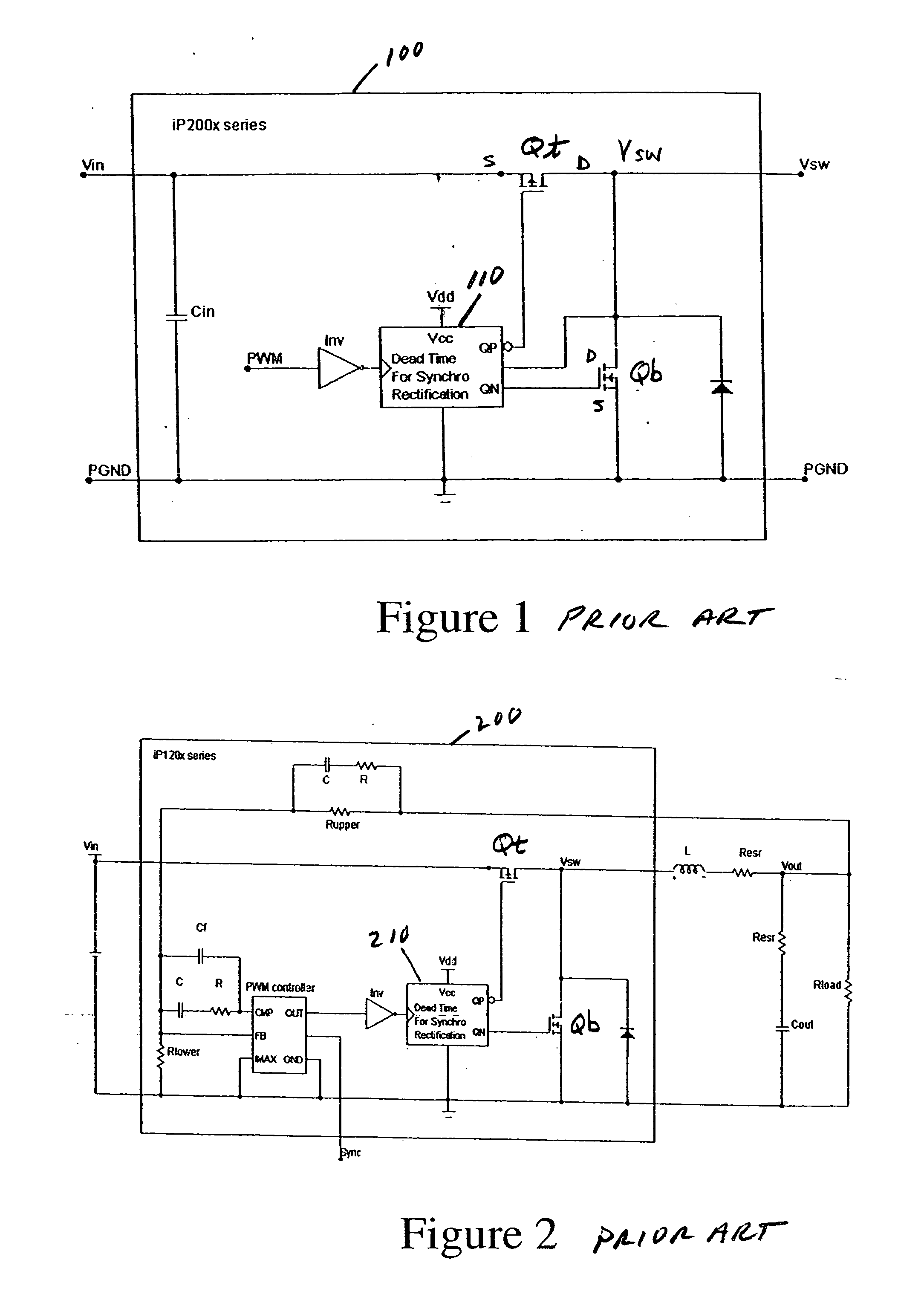
[0034] The first issue has been resolved by the test circuit shown in FIG. 3 having an external FET to charge the current on the avalanche inductor La.

[0035] The second issue has been resolved by pre-charging the input cap Cin to the BVdss of the top FET Qt. Also a diode Da is used in the avalanche circuit (FIG. 3) to avoid the cap Cin being discharged.

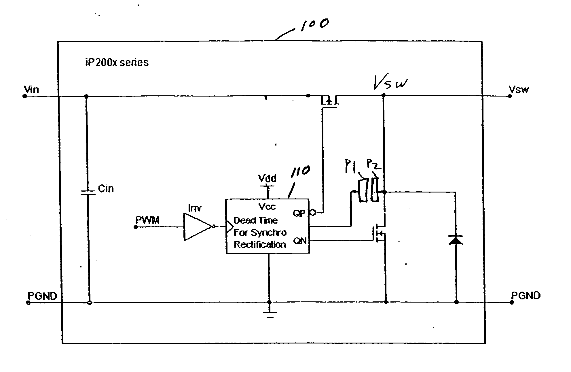
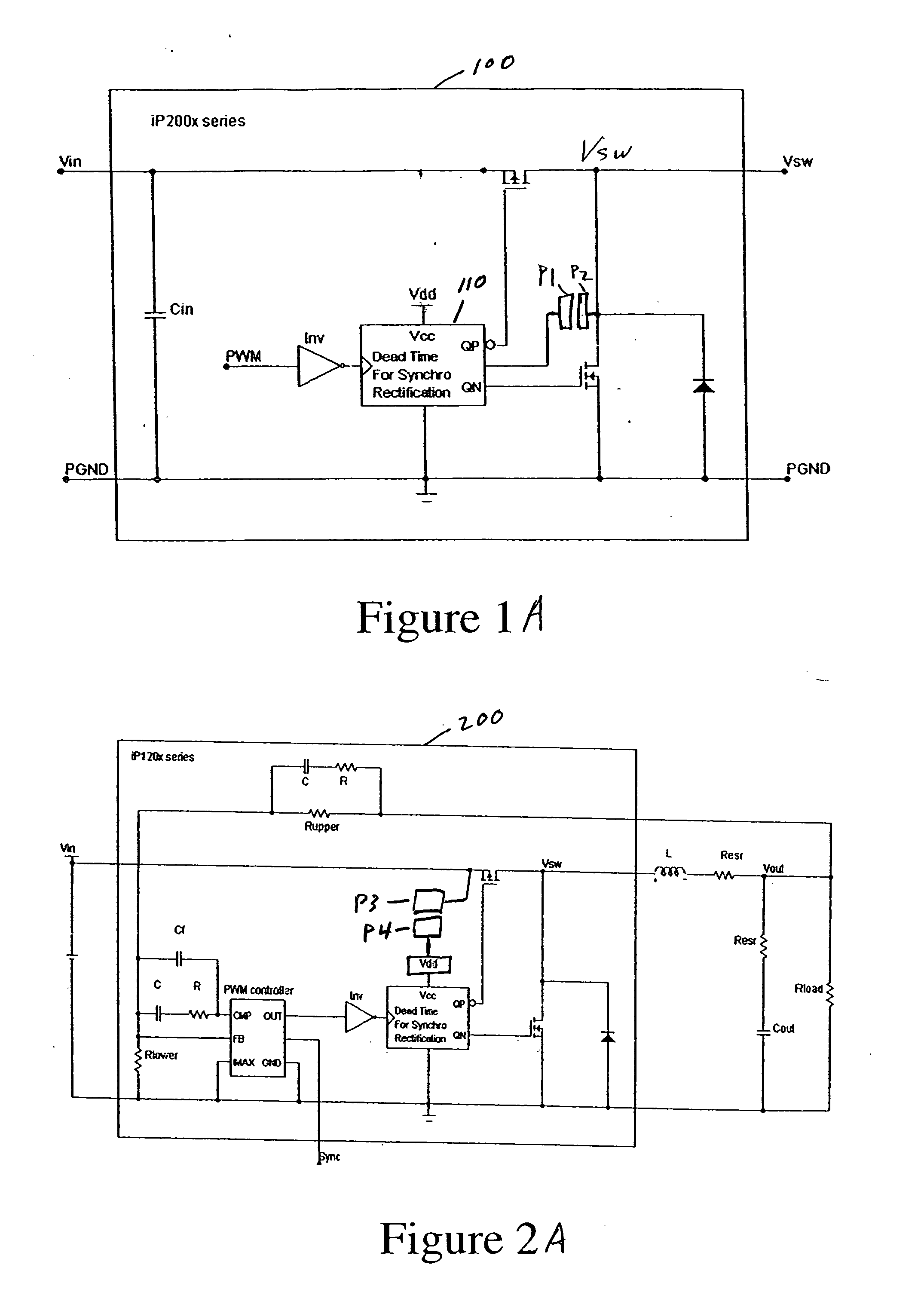
[0036] The third issue has been resolved by splitting the internal pad (not shown) connecting the switch node Vsw to the IC 110, forming pads P1 and P2. See FIG. 1A. In this way the IC 110 doesn't see the high voltage applied to the bottom FET Qb. Also we supply 20V on the switch node Vsw which brings the gate of the top FET up to 20V and we can run avalanche testing on bottom FET Qb assuming that the BVdss is lower than 40V. The two pads P1, P2 are shown schematically and need not be located at any specific part of the module 100. They are externally accessible. When installed in a complete converter circuit, the pads P1, P2 are co...


PUM


Abstract

An avalanche test circuit for applying an avalanche test signal to a device under test, comprising a series combination of a voltage source and an inductance; a switching device connected in parallel with said series combination; a diode for being connected to a test terminal of said device under test, said diode being connected to a connection point of said inductance and said switching device; a common terminal of said device under test being connected to a connection point of said switching device and said voltage source.

Description

CROSS-REFERENCE TO RELATED APPLICATION [0001] This application is based upon and claims priority of U.S. Provisional Ser. No. 60 / 647,986 filed Jan. 28, 2005, incorporated by reference.BACKGROUND OF THE INVENTION [0002] 1. Field of the Invention [0003] A method and device for avalanche testing of top and bottom FETs of a DC to DC buck converter. [0004] 2. Background Art [0005] In the last few years it has become very critical to screen defective devices before the final assembly of a module in order to reduce cost. [0006] Known Good Die (KGD) test systems using probes and / or pogo pin contacts are available to guarantee that only good dies will be assembled in the final module, although these systems can be expensive. [0007] However, a critical test that is difficult to implement using a probe is the avalanche test. All semiconductor devices are rated for a certain maximum reverse voltage (BVdss for power MOSFETs). Operation above this threshold will cause high electric fields in reve...

Claims


Application Information

Patent Timeline
IPC IPC(8): G01R31/02H01J40/14G01J1/44
CPCG01R31/2621G01R31/40
Inventor CIUFFOLI, ANDREA
Owner INFINEON TECH AMERICAS CORP
Why Eureka
Try Eureka