Compact antenna

a compact antenna and antenna element technology, applied in the direction of resonant antennas, antenna earthings, protective materials radiating elements, etc., can solve the problems of difficult to maintain the required wide-band characteristics, difficult to realize the reduction of the size of the antenna element with maintaining the wide-band characteristics, and difficult to find appropriate design conditions which maintain the wide-band characteristics. achieve the effect of reducing the size of the antenna element, and adjusting the impedan

Inactive Publication Date: 2006-08-10
FURUKAWA ELECTRIC CO LTD
View PDF3 Cites 20 Cited by
  • Summary
  • Abstract
  • Description
  • Claims
  • Application Information

AI Technical Summary

Benefits of technology

[0041] According to the present invention, in addition to the effect mentioned above, it is possible to easily adjust the impedance for adjusting the resonant frequencies and broadening the frequency bands.
[0042] According to the present invention, since the dielectric having three-layer structure and the fed element and the grounded parasitic element are combined, and each conducting element is configured so as to have folded antenna elements by connecting line conductors, it is possible to realize the multi-band antenna which, with maintaining the broad band properties obtained by the effect of electromagnetic coupling, enables to reduce its size and to make low-profile and is suitable to be built inside the mobile terminals.

Problems solved by technology

However, if the size of the antenna is reduced regardless of being a line antenna or planar one, it is difficult to maintain the required wide-band characteristics.
Especially, adopting the method for reducing the size of the antenna by increasing the dielectric constant of the dielectric material surrounding the whole antenna makes it difficult to find appropriate design conditions which maintain the wide-band characteristics.
Thus, the configuration of the prior art has a problem, for the use of the multi-band antenna which can be built inside a mobile terminal, that it is difficult to realize the reduction of the size of the antenna element with maintaining the wide-band characteristics.

Method used


Image

  • Compact antenna
  • Compact antenna
  • Compact antenna

Examples


first embodiment

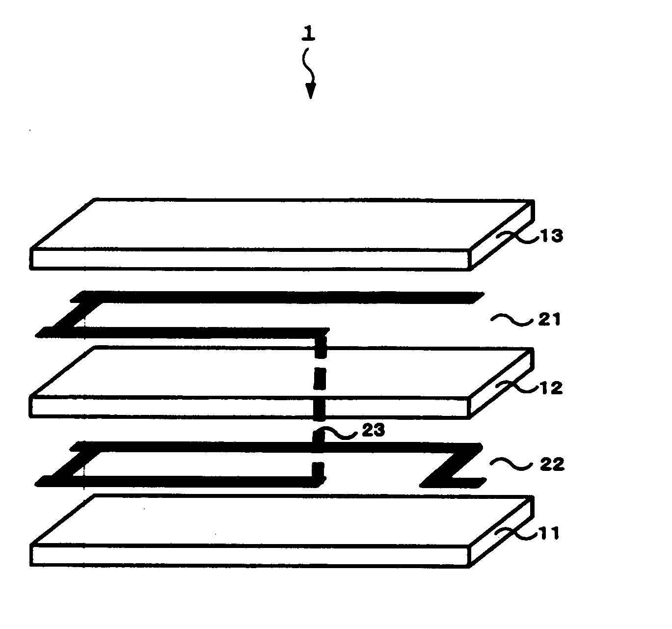
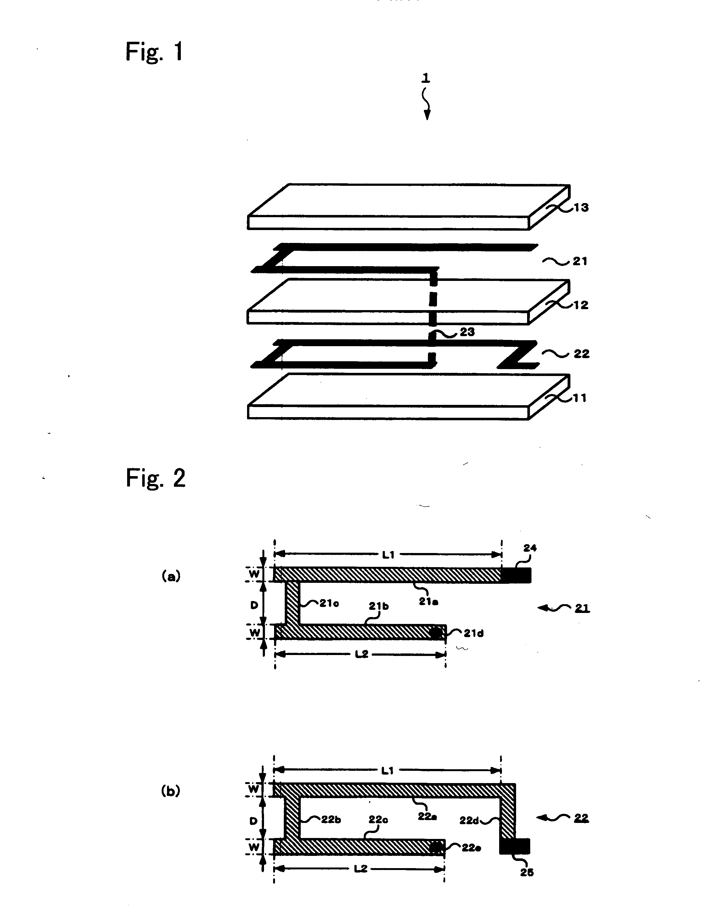
[0061] The configuration of the multi-band antenna in accordance with a first embodiment of the present invention will be explained first with referring to accompanying drawings. FIG. 1 is a perspective view that illustrates the structure of the multi-band antenna in accordance with the first embodiment. And, FIG. 2 is a schematic view that illustrates the configuration of the antenna elements of the multi-band antenna shown in the FIG. 1.

[0062] As illustrated in FIG. 1, the multi-band antenna 1 in accordance with the first embodiment has a stacked-layer structure which is obtained by stacking three layers consisting of a first dielectric layer 11, a second dielectric layer 12, and a third dielectric layer 13 in this order from the bottom side. Moreover, a fed element 21 is formed as an antenna element between the second dielectric layer 12 and the third dielectric layer 13, and a grounded parasitic element 22 is formed between the first dielectric layer 11 and the second dielectri...

second embodiment

[0093] Hereinafter, the configuration of the multi-antenna in accordance with the second embodiment will be explained, with reference to accompanying drawings. Since the basic configuration of the multi-band antenna is common to that of the first embodiment and the second embodiment, detail explanation is omitted. On the other hand, in the second embodiment, the way of mounting the multi-band antenna on the circuit board is different from that of first embodiment.

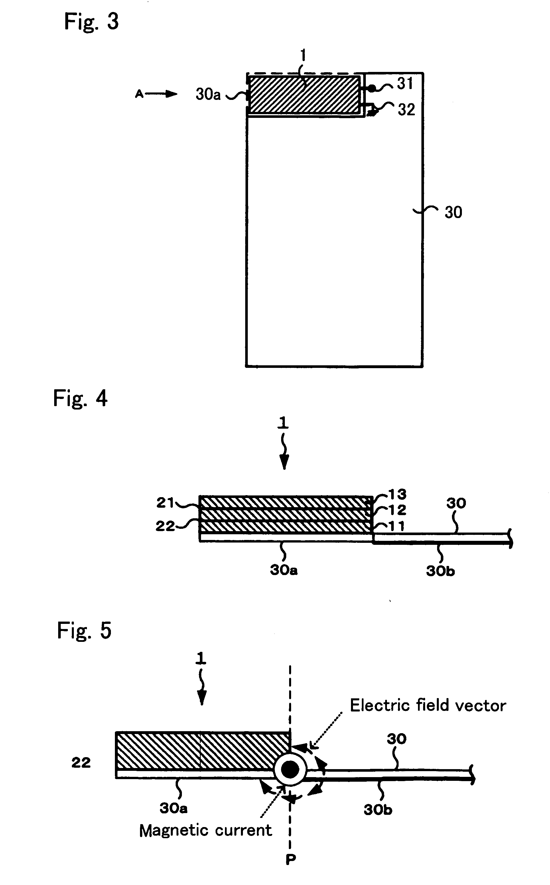
[0094]FIG. 10 is a side view that illustrates the state of the multi-band antenna 2 mounted on the circuit board 70 with a similar manner shown in the FIG. 4. The circuit board 70 shown in FIG. 10 is similar to the circuit board 30 illustrated in FIG. 3, and has a notch portion 70a obtained by removing a portion of the ground conductor 70b. Hereat, while, in the first embodiment, an arrangement is made so as that each layer of the multi-band antenna 1 is parallel to the face of the circuit board 30, in the second embodimen...

third embodiment

[0101] The configuration of the multi-band antenna in accordance with the third embodiment is explained hereinafter, with reference to the accompanying drawings. In the third embodiment, since the basic configuration is also common to that of the first embodiment, the detail explanation is omitted for the brevity and / or the clarity. In the third embodiment, in order to obtain three band operations, the fed element and grounded parasitic element are configured with line conductors folded in triple row.

[0102] FIGS. 12(a) and (b) illustrate, respectively, the fed element 91 and grounded parasitic element 92 in accordance with the third embodiment. The fed element 91 and grounded parasitic element 92 have elements consisting of line conductors in triple row each of which is obtained by folding the line conductor near the place opposite to the feed port 93 or ground port 94 and folding further near the place of the feed port 93 or ground port 94, wherein among the line conductors in tri...


PUM


Abstract

The multi-band antenna 1 is provided with a dielectric having the three-layer structure obtained by stacking layers so as that a central dielectric layer 12 made of a low dielectric constant material is sandwiched by lower and upper side dielectric layers 11, 13 made of high dielectric constant materials, a fed element 12 formed between the central dielectric layer 12 and the upper dielectric layer 13 and its base end being connected to a feed point on a specified side face of the dielectric having the three-layer structure, a grounded parasitic element 22 formed between the central dielectric layer 12 and the lower dielectric layer 11 and its base end being grounded on a specified side face, wherein the fed element 21 and the grounded parasitic element 22 is formed from the base end to the open end by a element obtained by connecting a plurality of line conductors and folding at least around the side face opposite to the specified face.

Description

CROSS-REFERENCE TO RELATED APPLICATIONS [0001] This application is a continuation of international patent application PCT / JP04 / 013415, filed Sep. 15, 2004, which is based upon and claims the benefit of priority from prior Japanese Patent Application No. 2004-116116, filed Apr. 4, 2004, the entire contents of each are incorporated herein by reference.FIELD OF THE INVENTION [0002] The present invention relates predominantly to a multi-band antenna commonly available in a plurality of frequency bands, especially, to the multi-band antenna of which the size can be reduced so as to be built inside such as mobile terminals. BACKGROUND TO THE INVENTION [0003] Recently, the use of mobile terminals such as mobile phones is widely spread, which has made it important to reduce the size of the antenna used in mobile terminals in order to make these mobile terminals small. Especially, antennas which can completely be built inside the mobile terminals without protruding from the mobile terminals ...

Claims


Application Information

Patent Timeline
Patent Type & Authority Applications(United States)
IPC IPC(8): H01Q1/38H01Q1/24H01Q1/36H01Q1/40H01Q5/10H01Q9/42
CPCH01Q1/243H01Q5/357H01Q1/40H01Q1/362H01Q13/00H01Q1/38H01Q1/24
Inventor TAMAOKA, HIROYUKI
Owner FURUKAWA ELECTRIC CO LTD
Why Eureka
Try Eureka