Flat cell read only memory using common contacts for bit lines and virtual ground lines

a read only memory and common contact technology, applied in the field of flat cell rom structure, can solve the problem of increasing the circuit area of the memory, and achieve the effect of speeding up the operation of the memory without increasing the layout area, reducing the height of the memory, and reducing the density of conta

Inactive Publication Date: 2006-08-10
ELAN MICROELECTRONICS CORPORATION
View PDF11 Cites 1 Cited by
  • Summary
  • Abstract
  • Description
  • Claims
  • Application Information

AI Technical Summary

Benefits of technology

[0009] With the first contact shared by two bits line and the second contact shared by two virtual ground lines, the contacts in a memory of the present invention are allowed to be slightly adjusted in their locations to insert a local word line for speeding up the operation of the memory without increasing the layout area. Moreover, in a memory of the present invention, with the first and second contacts shared by adjacent banks, the contact density is reduced, and the height of the memory is reduced accordingly.

Problems solved by technology

However, this solution requires a large number of additional word line drivers 12, thereby dramatically increasing the circuit area of the memory.

Method used


Image

  • Flat cell read only memory using common contacts for bit lines and virtual ground lines
  • Flat cell read only memory using common contacts for bit lines and virtual ground lines
  • Flat cell read only memory using common contacts for bit lines and virtual ground lines

Examples


Embodiment Construction

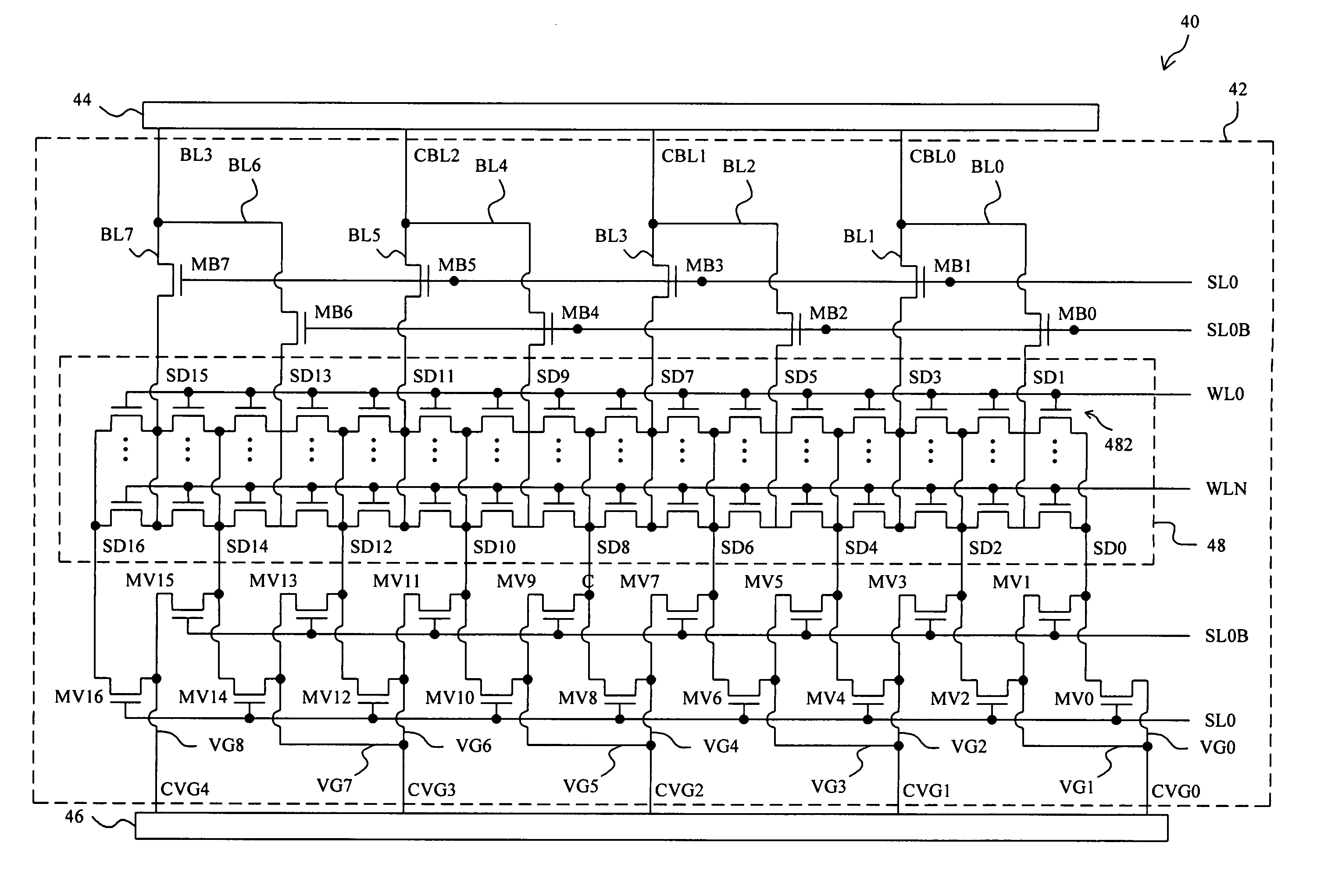
[0021]FIG. 5 shows a circuit diagram of a flat cell ROM 40 according to the present invention. In a memory bank 42 of the ROM 40, a memory array includes several transistors 482 serving as memory cells arranged in a manner that the gates of the transistors 482 on the same row are connected to a common word line among WL0-WLN, and the sources / drains of the transistor 482 on the same column are connected to one of bit lines BL0-BL7 or virtual ground lines VG0-VG8, respectively. The bit lines BL0 and BL1 are bonded together to a common bit line CBL0, and capable of being connected to the memory array 48 through transistors MB0 and MB1, respectively. The bit lines BL2 and BL3 are bonded together to a common bit line CBL1, and capable of being connected to the memory array 48 through transistors MB2 and MB3, respectively. The bit lines BL4 and BL5 are bonded together to a common bit line CBL2, and capable of being connected to the memory array 48 through transistors MB4 and MB5, respecti...


PUM


Abstract

In a flat cell read only memory, two bit lines or two virtual ground lines share a common contact such that the contact is slightly adjustable in its location for inserting a local metal word line without increasing the layout area to improve the reading speed of the memory. Moreover, two adjacent banks of the memory share common bit lines or virtual ground lines, whereby reducing the contact density and height of the memory.

Description

FIELD OF THE INVENTION [0001] The present invention is related generally to a read only memory (ROM) and more particularly to a flat cell ROM structure for high-speed applications. BACKGROUND OF THE INVENTION [0002] Speeding up is always one of the attempts in the ROM design. For a high-speed memory, the main bottleneck in design is the low speed on the word line owing to the large resistance and parasitic capacitance inherent in a polysilicon word line, and there have been proposed two solutions for improving thereto. The first one is to separate a word line into several segments along the length thereof, and provide for each segment of the word line with an individual word line driver, so as to have a higher operating speed of the memory. In other words, the memory is separated into several small ones in this solution. For more illustrative, FIG. 1 is a schematic diagram of this solution, in which FIG. 1A is a simplified diagram of showing several word lines 10 and word line drive...

Claims


Application Information

Patent Timeline
Patent Type & Authority Applications(United States)
IPC IPC(8): G11C8/00
CPCG11C17/126H01L27/0207H01L27/112H01L27/1122H10B20/30H10B20/00
Inventor CHEN, HSU-SHUN
Owner ELAN MICROELECTRONICS CORPORATION
Why Eureka
Try Eureka