Semiconductor Device with Improved Contact Structure and Method of Forming Same

a technology of a semiconductor device and a contact structure, which is applied in the direction of semiconductor devices, semiconductor/solid-state device details, electrical devices, etc., can solve the problems of limiting device performance in various ways, affecting the efficiency of the device, so as to reduce the contact density, improve the process window, and reduce the aspect ratio

Active Publication Date: 2009-01-15
MOSAID TECH
View PDF10 Cites 109 Cited by
  • Summary
  • Abstract
  • Description
  • Claims
  • Application Information

AI Technical Summary

Benefits of technology

[0009]These and other problems are generally solved or circumvented, and technical advantages are generally achieved, by preferred embodiments of the present invention which provide a contact structure where a contact to a MOS transistor comprises a first contact formed in a first dielectric layer, in contact with a source / drain region, and a second contact formed in a second dielectric layer, connecting to a gate region or a preformed first contact. A butted contact structure abutting a source / drain of a first transistor and the gate region of a second transistor comprises a first contact formed in a first dielectric layer, in contact with a source / drain region of the first transistor, and a second contact formed in a second dielectric layer, having one end resting on the gate electrode of the second transistor and the other end in contact with the preformed first contact. The advantageous features of the contacts in preferred embodiments include reduced aspect ratio and reduced contact density, which may lead to improved process window and enhanced device yield.

Problems solved by technology

However, as transistor dimensions continue to scale down in advanced processing technology, this and other prior art contact structures begin to limit device performance in various ways.
Cutting contact openings having an aspect ratio of this level will typically take a much longer time, compared with the dry etch process used in forming the contact openings in the prior art.
A detrimental effect known as “striation” may also occur on the surface region between adjacent contact holes due to severe photoresist losses on the edges of the contact openings during the long plasma etch process.
“Striation” causes electrical shorting between adjacent contacts and may cause severe device yield loss.
This problem is compounded by the increased contact opening density on a wafer surface processed using advanced technology.
However, a tapered contact opening with a very large aspect ratio may result in a substantially reduced contact landing area on the source / drain region and gate electrode.
This may, in turn, lead to a substantial increase in contact resistance and deteriorated device performance.
A reduced margin for misalignment may cause substantial device yield loss or create serious device reliability concerns, especially in a butted contact area, where a misalignment may easily cause a complete disconnection to a diffusion region or a gate electrode.

Method used


Image

  • Semiconductor Device with Improved Contact Structure and Method of Forming Same
  • Semiconductor Device with Improved Contact Structure and Method of Forming Same
  • Semiconductor Device with Improved Contact Structure and Method of Forming Same

Examples


Embodiment Construction

[0023]The making and using of the presently preferred embodiments are discussed in detail below. It should be appreciated, however, that the present invention provides many applicable inventive concepts that can be embodied in a wide variety of specific contexts. The specific embodiments discussed are merely illustrative of specific ways to make and use the invention, and do not limit the scope of the invention.

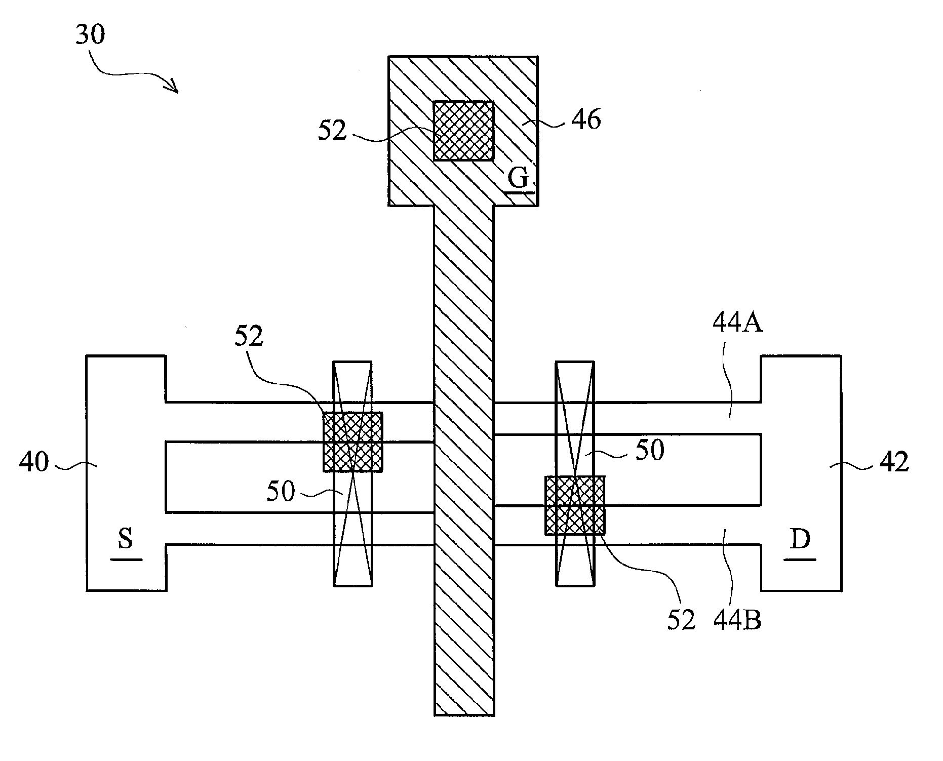
[0024]The present invention will be described with respect to preferred embodiments in a specific context, namely an improved contact structure and the method of forming the same. This inventive contact structure comprises a first type connecting to the source / drain regions of MOS transistors, having a bottom and top portion. The contact structure also comprises a second type connecting to either the contacts of the first type or gate electrodes of MOS transistors. This contact structure exhibits the desired contact characteristics for the advanced technology generation. The ...


PUM


Abstract

A contact structure includes a first contact formed in a first dielectric layer connecting to the source / drain region of a MOS transistor, and a second contact formed in a second dielectric layer connecting to a gate region of a MOS transistor or to a first contact. A butted contact structure abutting a source / drain region and a gate electrode includes a first contact formed in a first dielectric layer connecting to the source / drain region of a MOS transistor, and a second contact formed in a second dielectric layer with one end resting on the gate electrode and the other end in contact with the first contact.

Description

TECHNICAL FIELD[0001]The present invention relates generally to semiconductor integrated circuits, and more particularly, to semiconductor devices having improved contact structure.BACKGROUND[0002]Contacts are typically vertical metal interconnect structures formed in an integrated circuit that connect the diffusion regions and gate electrodes of a semiconductor device to the first layer of interconnect. Individual semiconductor devices formed in a semiconductor substrate are usually electrically coupled to each other through contacts in order to form functional integrated circuits. The desired characteristics of a contact include a minimum contact resistance, ease of fabrication, and good reliability.[0003]FIG. 1 shows a cross sectional view of a semiconductor device employing the conventional self-aligned silicide, tungsten plug contact configuration. In forming this prior art contact structure, after the creation of transistors is complete, a silicide layer 5 is deposited and pat...

Claims


Application Information

Patent Timeline
Patent Type & Authority Applications(United States)
IPC IPC(8): H01L27/01H01L21/84H01L29/94
CPCH01L27/11H01L27/1104H01L23/528H01L27/0207H01L23/485H01L23/522H01L2924/0002H01L23/5226H01L23/5283H01L2924/00H01L21/76895H01L29/41791H10B10/00H10B10/12H01L21/32115H01L21/768H01L21/823425H01L21/823437H01L21/823475H01L27/088H01L29/0649H01L29/66568
Inventor LIAW, JHON-JHY
Owner MOSAID TECH
Why Eureka
Try Eureka