
Eureka
For R&D, Eureka makes reading and utilizing patents & technical documents easy.
Eureka AIR
Designed for self-driven R&D workflows. Generate viable solutions, solve complex R&D challenges, empower your innovation with AI.

Eureka Materials
Designed for material experts only. Revolutionize your material R&D, from search, analyze, to developing new materials.

TechResearch
Generate reliable direction feasibility study reports for your R&D in just a few steps.

TechSeek
Discover and master advanced knowledge NOW. Basics, ideas, possibilities, all at once.

TechMind
As an expert in R&D Theories, TechMind can generates customized viable solutions instantly.

TechRisk
Analyze your overall solution with one click, know your potential R&D risks in advance.

TechMonitor
Get weekly tech updates, stay abreast of the latest tech innovations and key insights.
TFT substrate for display device and manufacturing method of the same
- Summary
- Abstract
- Description
- Claims
- Application Information
AI Technical Summary
Benefits of technology
Problems solved by technology
Method used
Image

Examples
first embodiment
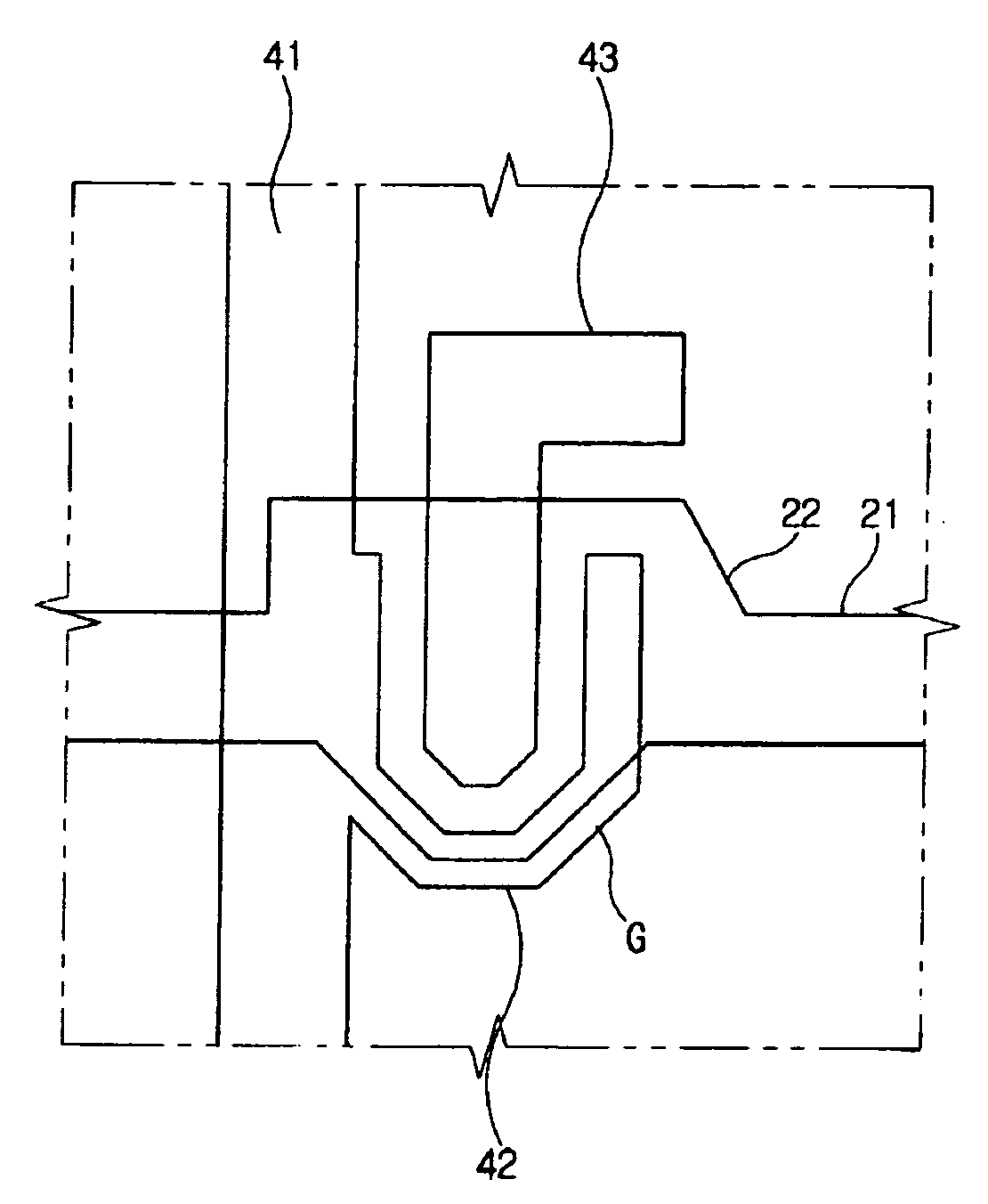
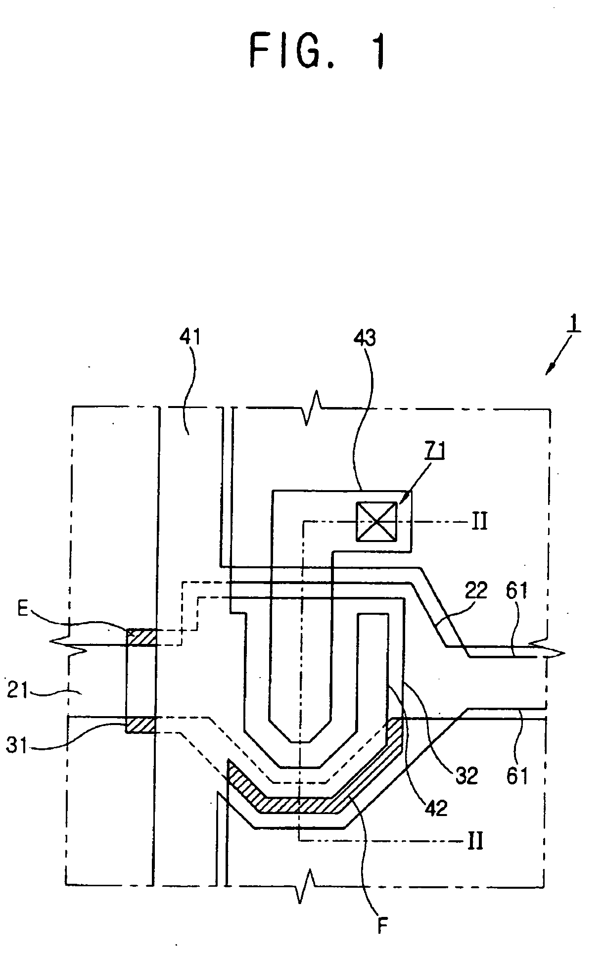
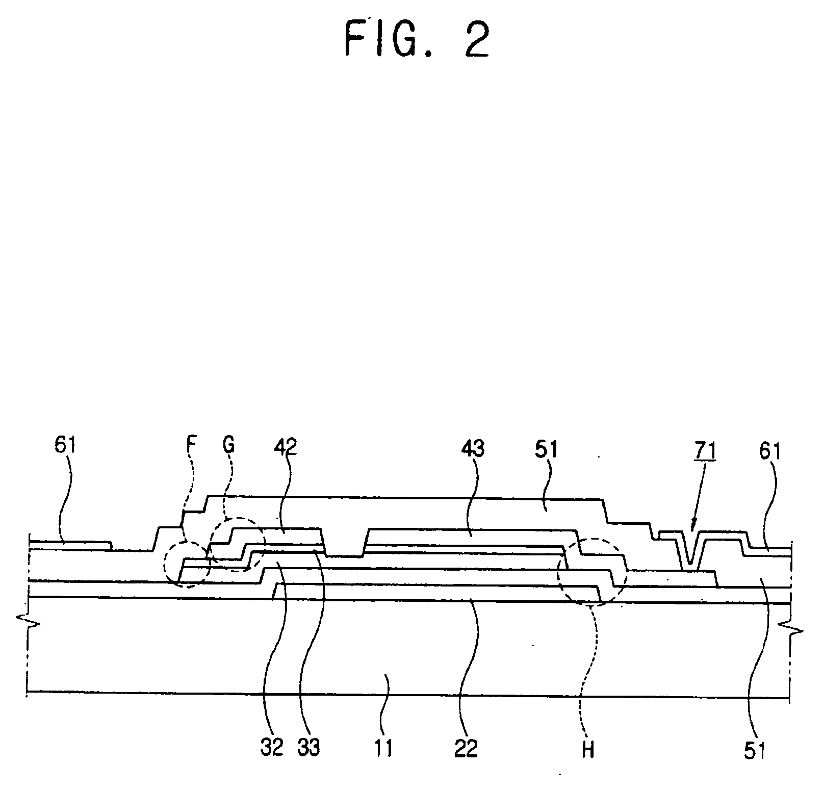
[0028] A TFT substrate 1 will be described below by referring to FIGS. 1 to 5.
[0029] Referring now to FIGS. 1 to 4, a gate wiring 21 and 22 is formed on an insulating substrate 11. The gate wiring 21 and 22 comprises a gate line 21 extending in a transverse direction and a gate electrode 22 connected to the gate line 21.
[0030] A gate insulation layer 31 made of, for example, silicon nitride (SiNx), is formed on the insulating substrate 11 and covers the gate wiring 21 and 22.
[0031] A semiconductor layer 32 made of, for example, amorphous silicon, is formed on the gate insulation layer 31 of the gate electrode 22. An ohmic contact layer 33 made of, for example, silicide or n+ hydrogenated amorphous silicon heavily doped with n-type impurity, is formed on the semiconductor layer 32.
[0032] A data wiring 41, 42, and 43 is formed on the ohmic contact layer 33 and the gate insulation layer 31. The data wiring 41, 42, and 43 may have a Mo single-layered structure or a Mo / Al / Mo triple-l...
second embodiment
[0053] A TFT substrate will be described below with reference to FIGS. 9 and 10.
[0054] Unlike the first embodiment, a whole source electrode 42 overlaps a gate electrode 22. Like the first embodiment, the whole semiconductor layer 32 under a drain electrode 43 overlaps the gate electrode 22, and a semiconductor layer 32 under the source electrode 42 extends outward from the gate electrode 22.
[0055] According to the second embodiment, an area where the source electrode 42 and the gate electrode 22 overlap becomes larger, thereby increasing RC delay. However, the size of the gate electrode 22 becomes smaller than in a full island structure, thereby enhancing the aperture ratio. Moreover, a leakage current directed from the drain electrode 43 to the source electrode 42 is not generated, thereby reducing afterimaging.
third embodiment
[0056] A TFT substrate will be described below with reference to FIGS. 11 and 12.
[0057] Unlike the first embodiment, a channel area has a straight shape. Like the first embodiment, a whole semiconductor layer 32 under a drain electrode 43 overlaps the gate electrode 22, and a semiconductor layer 32 under a source electrode 42 extends outward from the gate electrode 22.
[0058] According to the third embodiment, the size of the gate electrode 22 becomes smaller than in a full island structure, thereby enhancing the aperture ratio. Also, there is no leakage current directed from the drain electrode 43 to the source electrode 42, thereby reducing afterimaging.
[0059] The TFT and the TFT substrate according to the embodiment of the present invention can be employed in not only LCDs but also in organic light emitting diodes (OLEDs) Here, the OLED uses an organic material that emits light by itself when it receives an electric signal. Such an OLED having a layered structure comprises a ca...
PUM
 Abstract
Description
Claims
Application Information
 - R&D Engineer
- R&D Manager
- IP Professional
- Industry Leading Data Capabilities
- Powerful AI technology
- Patent DNA Extraction
Browse by: Latest US Patents, China's latest patents, Technical Efficacy Thesaurus, Application Domain, Technology Topic, Popular Technical Reports.
© 2024 PatSnap. All rights reserved.Legal|Privacy policy|Modern Slavery Act Transparency Statement|Sitemap|About US| Contact US: help@patsnap.com