Active pixel image sensors

a technology of image sensors and active pixel arrays, which is applied in the field of active pixel array image sensors, can solve the problems of poor suited cmos fabrication techniques for the formation of active pixel arrays of cis devices, prone to signal degradation and noise induced errors,

Inactive Publication Date: 2006-08-24
SAMSUNG ELECTRONICS CO LTD
View PDF14 Cites 45 Cited by
  • Summary
  • Abstract
  • Description
  • Claims
  • Application Information

AI Technical Summary

Problems solved by technology

Nevertheless, CMOS fabrication techniques are not well suited to the formation of the active pixel array of CIS devices.
Such analog interfaces, however, are prone to signal degradation and noise induced errors.

Method used


Image

  • Active pixel image sensors
  • Active pixel image sensors
  • Active pixel image sensors

Examples


Embodiment Construction

[0019] The present invention will now be described by way of several preferred but non-limiting embodiments.

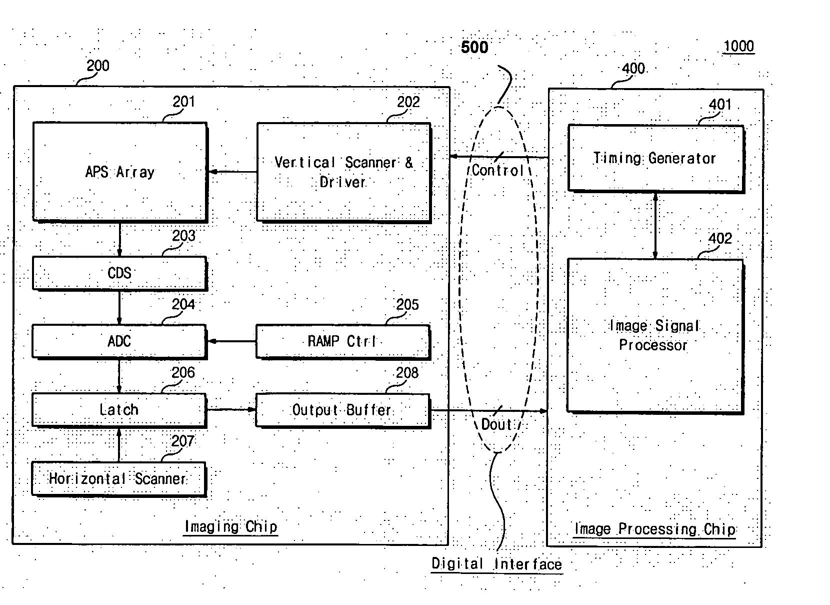
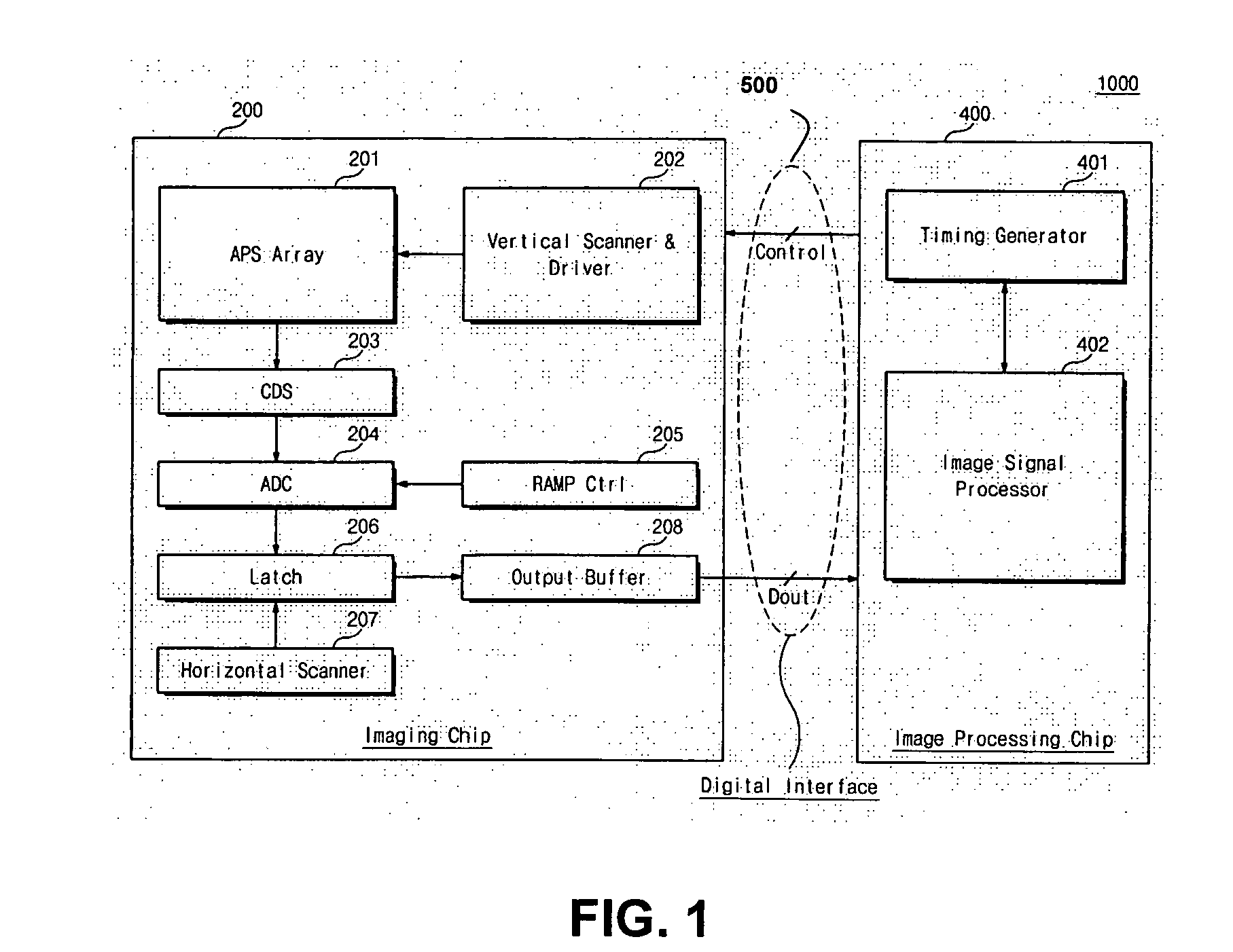
[0020]FIG. 1 is a schematic block diagram of an image sensor 1000 according to an embodiment of the present invention. As illustrated, the image sensor 1000 of this example includes first and second semiconductor chips 200 and 400 operatively coupled by a digital interface 500. The first chip 200 is an imaging chip which includes image sensors and related control circuits, while the second chip 400 is an image processing chip which generally includes image signal processing and timing circuits. Although the invention is not so limited, the chips 200 and 400 can be mounted side-by-side, or stacked one over the other, on a printed circuit board (PCB) or the like.

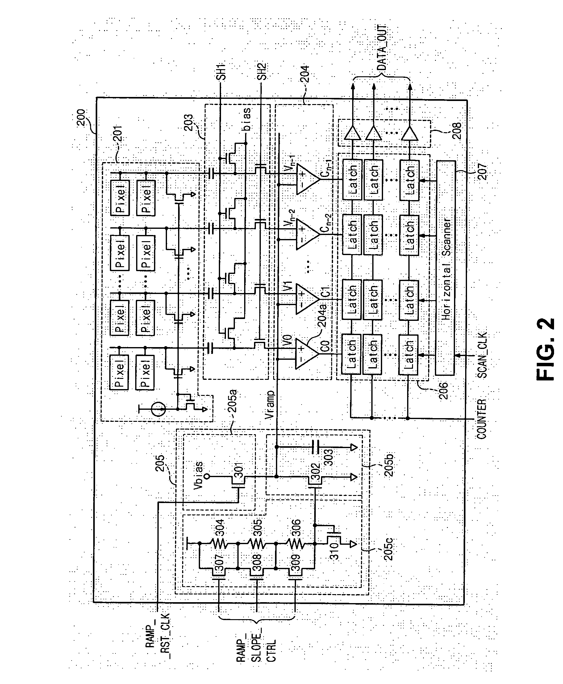
[0021] Still referring to FIG. 1, the imaging chip 200 of this embodiment includes active pixel sensor (APS) array 201, a vertical scan / drive circuit 202, a correlated double sampling (CDS) circuit 203, an analog-to-di...


PUM


Abstract

In one aspect, an imaging device is provided which includes first and second semiconductor chips and a digital interface. The first semiconductor chip includes an active pixel sensor, a digital input / output, and a plurality of control circuits, where transistors of the active pixel sensor are all n-type or p-type transistors, and where at least one of the controls circuits operates under control of a timing signal externally input to the digital input / output. The second semiconductor chip includes a timing generator which supplies the timing signal to the digital input / output of the first semiconductor chip. The digital interface is operatively connected between the digital input / output of first semiconductor chip and the second semiconductor chip.

Description

BACKGROUND OF THE INVENTION [0001] 1. Field of the Invention [0002] The present invention generally relates to the field of semiconductor devices, and more particularly, the present invention relates to image sensors having active pixel arrays. [0003] 2. Description of the Related Art [0004] Certain types of image sensors utilize photo conversion elements, such as photodiodes, to capture incident light and convert the light to an electric charge capable of image processing. Examples include Charge Coupled Device (CCD) image sensors and Complimentary Metal Oxide Semiconductor (CMOS) image sensors (CIS). The CCD image sensor is generally configured by an array of photo-detectors that are electrically connected to vertical CCDs functioning as analog shift registers. The vertical CCDs feed a horizontal CCD which in turn drives an output amplifier. In contrast, the CIS device is typically characterized by an array of photo detectors have access devices (e.g., transistors) for connection ...

Claims


Application Information

Patent Timeline
Patent Type & Authority Applications(United States)
IPC IPC(8): H01L27/00
CPCH01L27/14609H01L27/14634H04N5/335H04N25/00
Inventor LEE, KANY-BOKROH, JAE-SEOB
Owner SAMSUNG ELECTRONICS CO LTD
Why Eureka
Try Eureka