Solid-state imaging device

a solid-state imaging and imaging device technology, applied in the direction of picture signal generators, television systems, radioation controlled devices, etc., can solve the problems of affecting the miniaturization of the camera, increasing the manufacturing cost of the camera, etc., and achieve the effect of suppressing aliasing and reducing cos

Inactive Publication Date: 2006-08-24
FUJIFILM CORP
View PDF5 Cites 8 Cited by
  • Summary
  • Abstract
  • Description
  • Claims
  • Application Information

AI Technical Summary

Benefits of technology

[0019] According to the invention, in a solid-state imaging device structured such that photoelectric conversion layers are stacked above a semiconductor substrate,

Problems solved by technology

The stacked-type solid-state imaging device involves a problem that aliasing is generated likewise a single plate type solid-state imaging device.
While an optical low-pass filter is used in a cameral or the like, on which a single plate ty

Method used


Image

  • Solid-state imaging device
  • Solid-state imaging device
  • Solid-state imaging device

Examples


first embodiment

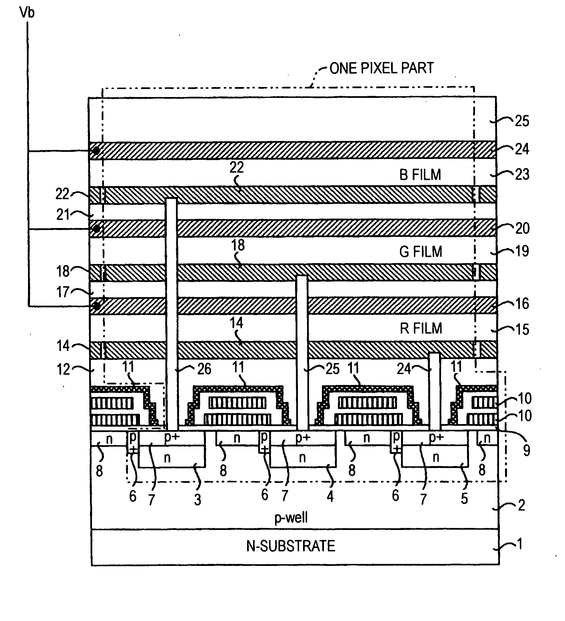
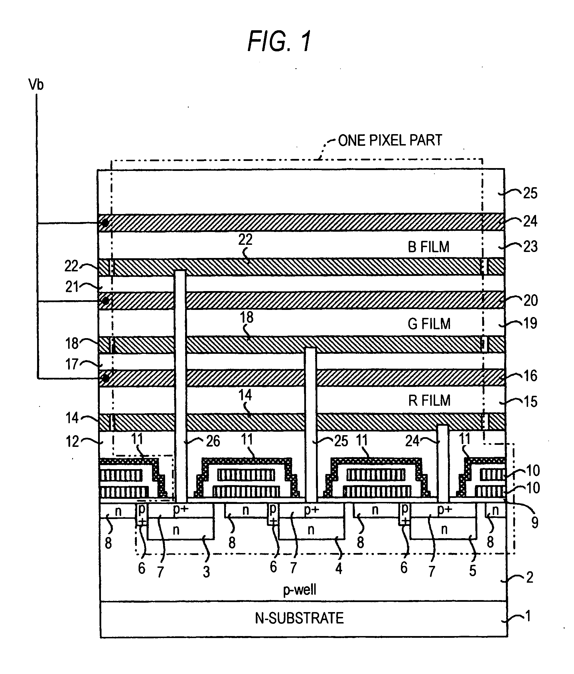
[0034]FIG. 1 is a schematic sectional view showing a fundamental structure of a pixel part of a solid-state imaging device to illustrate a first exemplary embodiment of the invention. A solid-state imaging device according to the embodiment includes pixel parts shown in FIG. 1 and arranged in a plurality of rows (for example, arranged in a square lattice).

[0035] As shown in FIG. 1, an R photoelectric conversion layer 15, which detects red (R) light and generates a red-color signal charge corresponding to the light, a G photoelectric conversion layer 19, which detects green (G) light and generates a green-color signal charge corresponding to the light, and a B photoelectric conversion layer 23, which detects blue (B) light and generates a blue-color signal charge corresponding to the light, are stacked in this order above a n-type semiconductor substrate 1. In addition, the number of and the order of stacking of the respective photoelectric conversion layers are not limited thereto....

second embodiment

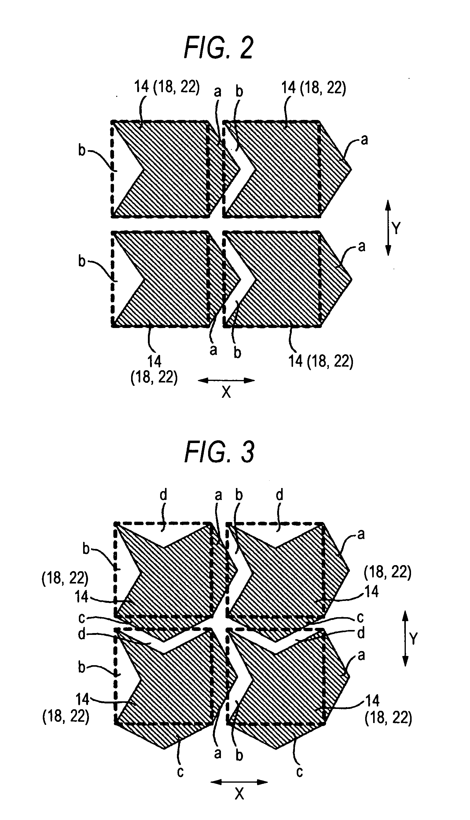
[0058] The fundamental structure of a solid-state imaging device to explain a second exemplary embodiment of the invention is substantially the same as that of the solid-state imaging device explained in the first embodiment. That is, with the structure, a signal charge generated in three pixel electrode layers stacked above a semiconductor substrate is once accumulated in an electric charge accumulating region provided on the semiconductor substrate and a signal corresponding to the signal charge accumulated therein is read to an outside with the use of VCCD and HCCD. However, the solid-state imaging device according to the second embodiment is structured such that at least one of the three pixel electrode layers included in one pixel part is divided into a plurality of sections, in which it is different from the first embodiment.

[0059]FIGS. 7A to 7D each is a plan view showing that pixel electrode layer included in the solid-state imaging device, by which the second embodiment of...


PUM


Abstract

A solid-state imaging device is provided and has a plurality of pixel parts including three photoelectric conversion layers stacked above a semiconductor substrate, the plurality of pixel parts being arranged above the semiconductor substrate. The three photoelectric conversion layers, respectively, included in one pixel part are interposed between pixel electrode layers and opposing electrode layers. A region thus interposed is made a pixel region that generates a signal charge for formation of one pixel data. The pixel region includes a convex portion and a concave portion as viewed in plane view, and a part of the convex portion is arranged in a manner to put in a concave portion in a pixel region of an adjacent pixel part.

Description

FIELD OF THE INVENTION [0001] The present invention relates to a solid-state imaging device, in which a plurality of pixel parts including a photoelectric conversion layer stacked on a semiconductor substrate are arranged on the semiconductor substrate. BACKGROUND OF THE INVENTION [0002] In the related art, a stacked-type solid-state imaging device described in, for example, JP-A-58-103165, JP-A-63-300575 and JP-A-2003-332551 is proposed as a solid-state imaging device structured such that any color filter is not used. With the stacked-type solid-state imaging device, three photoelectric conversion layers of an organic material and serving to detect, for example, red color (R), green color (G), and blue color (B) are stacked above a semiconductor substrate, signal charge generated in the respective layers is accumulated in a storage diode formed on the semiconductor substrate, and a signal readout circuit, such as vertical CCD, horizontal CCD, etc., formed on the semiconductor subst...

Claims


Application Information

Patent Timeline
IPC IPC(8): H01L29/04H01L27/146H04N5/335H04N5/369H04N9/07
CPCH01L27/14621H01L27/14812
Inventor MISAWA, TAKESHI
Owner FUJIFILM CORP
Why Eureka
Try Eureka