Phase change memory devices employing cell diodes and methods of fabricating the same

a phase change memory and cell diode technology, applied in semiconductor devices, digital storage, instruments, etc., can solve the problems of temporary instability of voltage induced to a bit line electrically connected to a selected phase change cell, voids or seams in isolation layers, and increase in the electrical resistance of word lines, etc., to achieve the effect of improving reliability and electrical characteristics

Active Publication Date: 2006-08-24
SAMSUNG ELECTRONICS CO LTD
View PDF9 Cites 114 Cited by
  • Summary
  • Abstract
  • Description
  • Claims
  • Application Information

AI Technical Summary

Benefits of technology

[0012] One embodiment of the present disclosure provides phase change memory devices that are suitable for improving reliability and electrical characteristics without degradation of integration density.
[0013] Another embodiment of the present disclosure provides methods of fabricating phase change memory devices that are capable of improving reliability and electrical characteristics without degradation of integration density.

Problems solved by technology

That is, the high aspect ratio of the deep trench regions may cause voids or seams in the isolation layer.
Over-etching of the word lines may cause an increase in the electrical resistance of the word lines.
When the current gain of the parasitic lateral bipolar transistor increases, a voltage induced to a bit line electrically connected to a selected phase change cell may be temporarily unstable during a read mode for reading data of the selected phase change cell.
As a result, access time for reading out data stored in the selected phase change cell may increase to degrade characteristics of the phase change memory device.
However, in the event that the thickness of the first N-type semiconductor layer is increased, the aspect ratio of the trench region may increase to degrade the reliability of the isolation layer in the trench region.

Method used


Image

  • Phase change memory devices employing cell diodes and methods of fabricating the same
  • Phase change memory devices employing cell diodes and methods of fabricating the same
  • Phase change memory devices employing cell diodes and methods of fabricating the same

Examples


Embodiment Construction

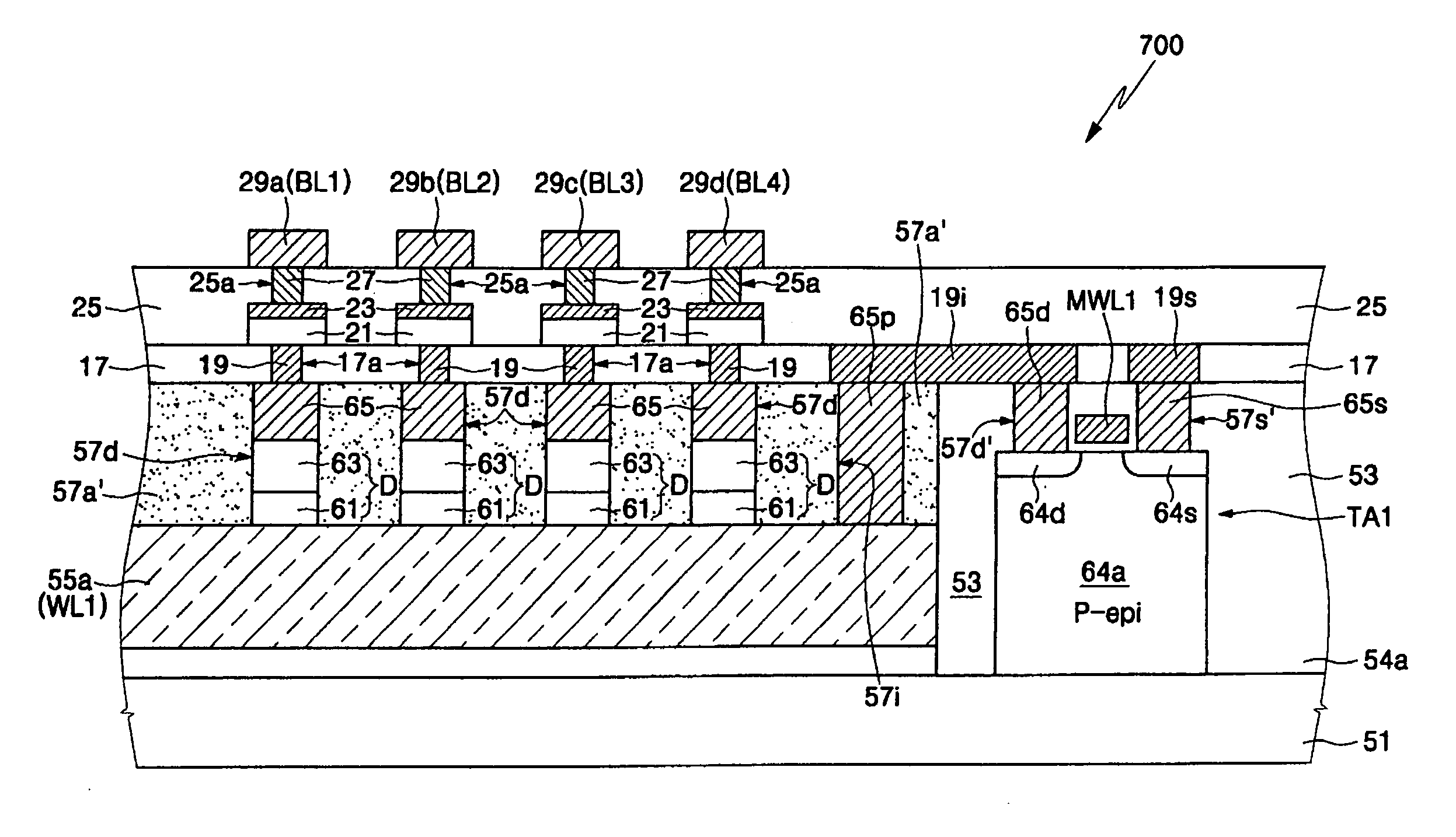
[0054] Exemplary embodiments of the present disclosure will be described in detail with reference to the accompanying drawings. The invention may, however, be embodied in many different forms and should not be construed as being limited to the embodiments set forth herein. Rather, these embodiments are provided so that this disclosure will be thorough and complete, and will fully convey the concept of the invention to those skilled in the art. In the drawings, lengths and thicknesses of layers and regions may be exaggerated for clarity. Like reference numerals in the drawings may denote like elements.

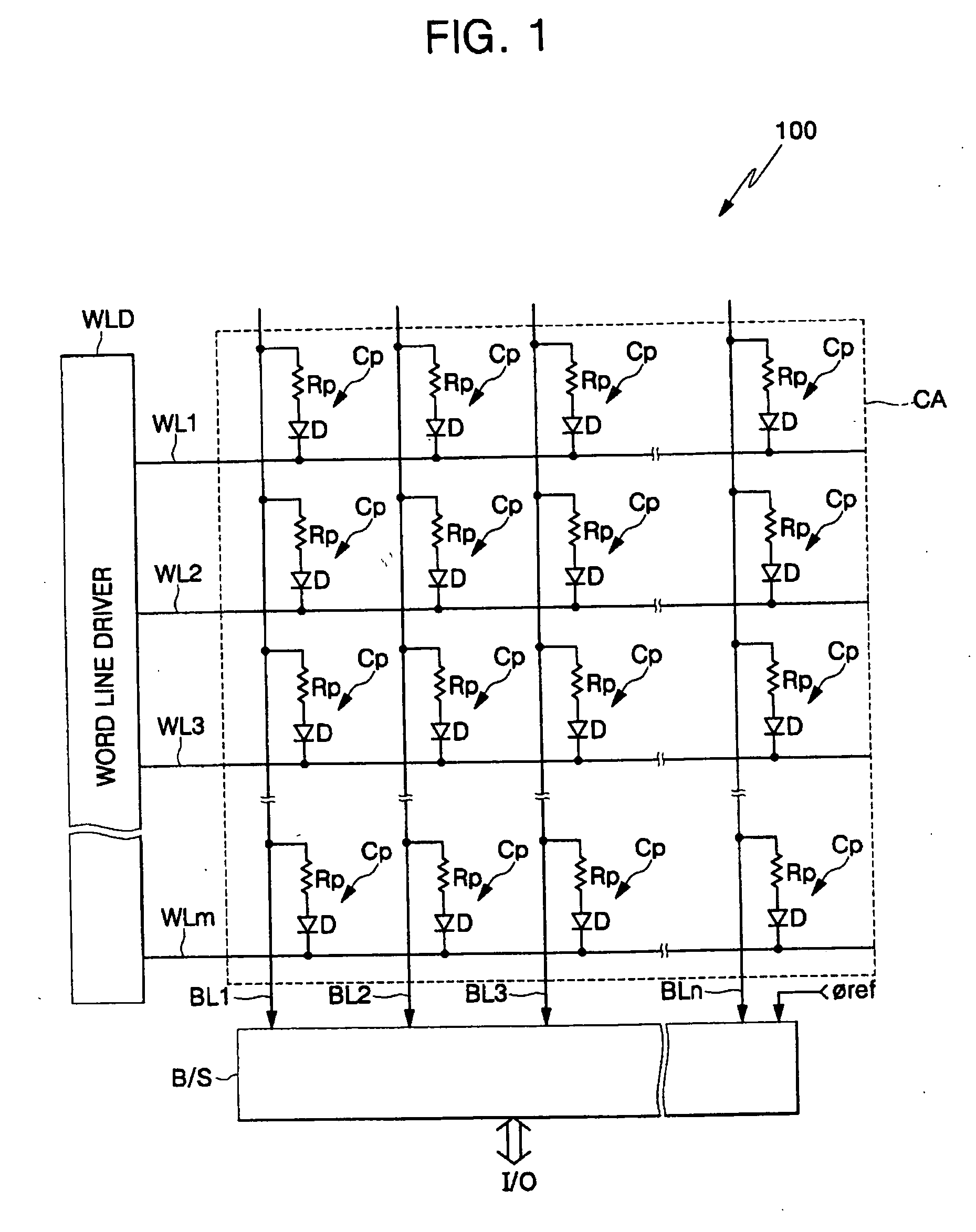
[0055]FIG. 1 is an exemplary block diagram illustrating a phase change memory device including phase change memory cells that employ cell diodes. The phase change memory device is indicated generally by the reference numeral 100.

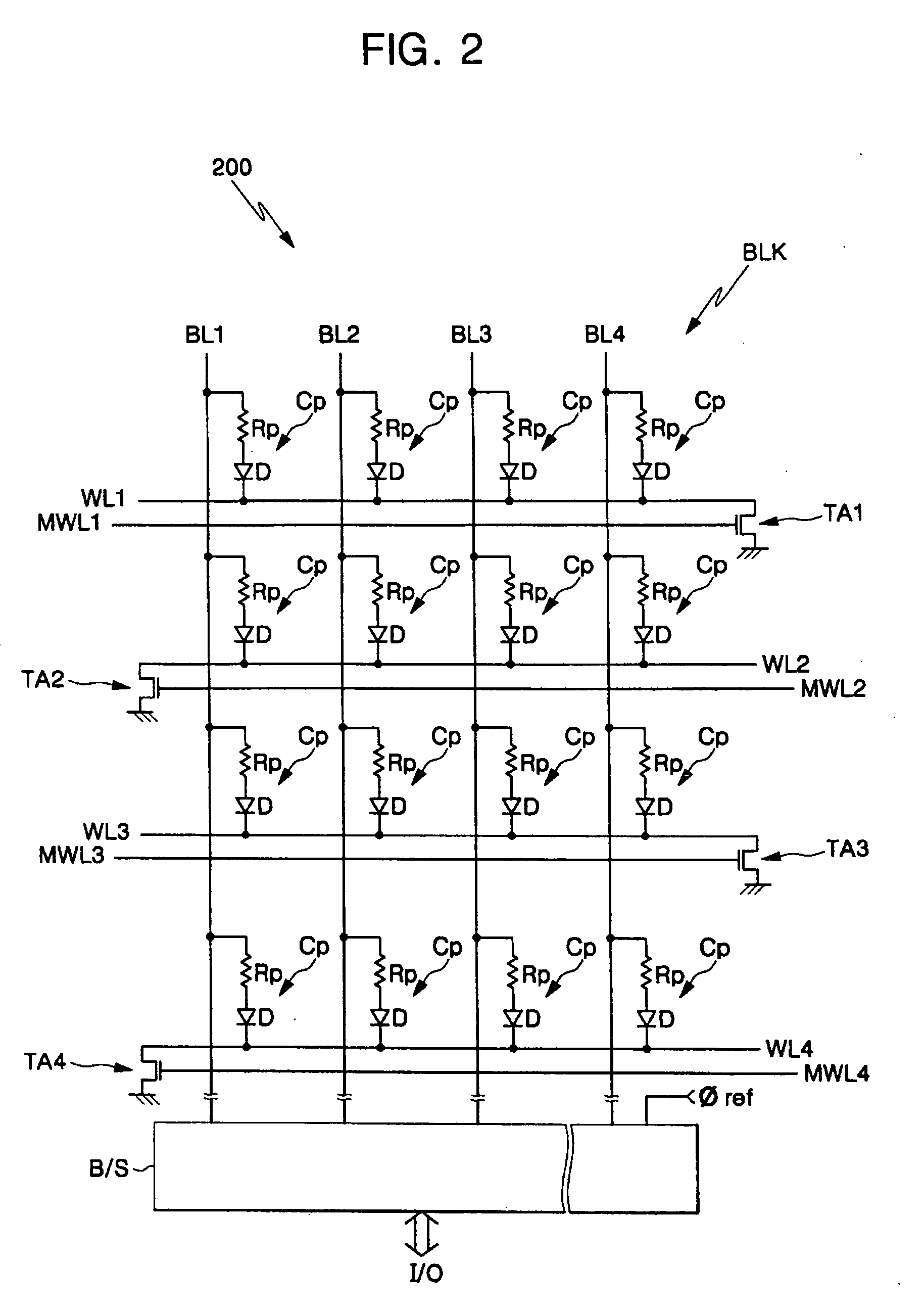
[0056] Referring to FIG. 1, the phase change memory device 100 includes a cell array region CA and a peripheral circuit region. The cell array region CA inclu...


PUM


Abstract

Phase change memory devices having cell diodes and related methods are provided, where the phase change memory devices include a semiconductor substrate of a first conductivity type and a plurality of parallel word lines disposed on the semiconductor substrate, the word lines have a second conductivity type different from the first conductivity type and have substantially flat top surfaces, a plurality of first semiconductor patterns are one-dimensionally arrayed on each word line along a length direction of the word line, the first semiconductor patterns have the first conductivity type or the second conductivity type, second semiconductor patterns having the first conductivity type are stacked on the first semiconductor patterns, an insulating layer is provided on the substrate having the second semiconductor patterns, the insulating layer fills gap regions between the word lines, gap regions between the first semiconductor patterns and gap regions between the second semiconductor patterns, a plurality of phase change material patterns are two-dimensionally arrayed on the insulating layer, and the phase change material patterns are electrically connected to the second semiconductor patterns, respectively.

Description

CROSS-REFERENCE TO RELATED APPLICATION [0001] This application claims foreign priority under 35 U.S.C. § 119 to Korean Patent Application No. 10-2005-0015564, filed on Feb. 24, 2005 in the Korean Intellectual Property Office, the disclosure of which is incorporated herein in its entirety by reference. BACKGROUND OF THE INVENTION [0002] 1. Field of the Invention [0003] The present disclosure relates to semiconductor memory devices and, more particularly, to memory devices employing cell diodes. [0004] 2. Description of Related Art [0005] Non-volatile memory devices have an advantage in that data stored in such memory cells does not vanish when electrical power is not supplied to the memory cells. The non-volatile memory devices mainly employ flash memory cells having a stacked gate structure. The stacked gate structure includes a tunnel oxide layer, a floating gate, an inter-gate dielectric layer and a control gate electrode, which are sequentially stacked on a channel region. Theref...

Claims


Application Information

Patent Timeline
Patent Type & Authority Applications(United States)
IPC IPC(8): H01L29/76
CPCG11C13/0004G11C2213/72H01L27/2409H01L27/2463H01L45/06H01L45/1233H01L45/1675H10B63/20H10B63/80H10N70/231H10N70/063H10N70/826H10N70/882
Inventor CHO, WOO-YEONGKIM, DU-EUNGSHIN, YUN-SEUNGBYUN, HYUN-GEUNKANG, SANG-BEOMCHO, BEAK-HYUNGKWAK, CHOONG-KEUN
Owner SAMSUNG ELECTRONICS CO LTD
Why Eureka
Try Eureka