
Land grid array package

a technology of grid arrays and packages, applied in the direction of printed circuit aspects, sustainable manufacturing/processing, final product manufacturing, etc., can solve the problems of power supply electrode disconnection and short circuit, short circuit, etc., and achieve the effect of further illustrating the operation and

Inactive Publication Date: 2006-08-24
SANYO ELECTRIC CO LTD +1
View PDF1 Cites 16 Cited by
  • Summary
  • Abstract
  • Description
  • Claims
  • Application Information

AI Technical Summary

Benefits of technology

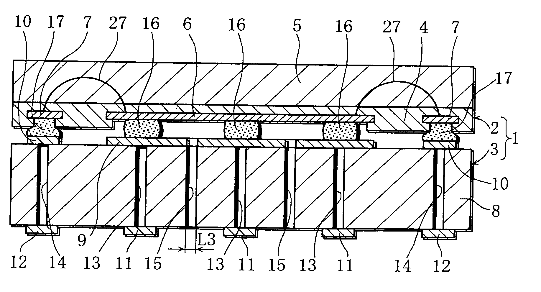
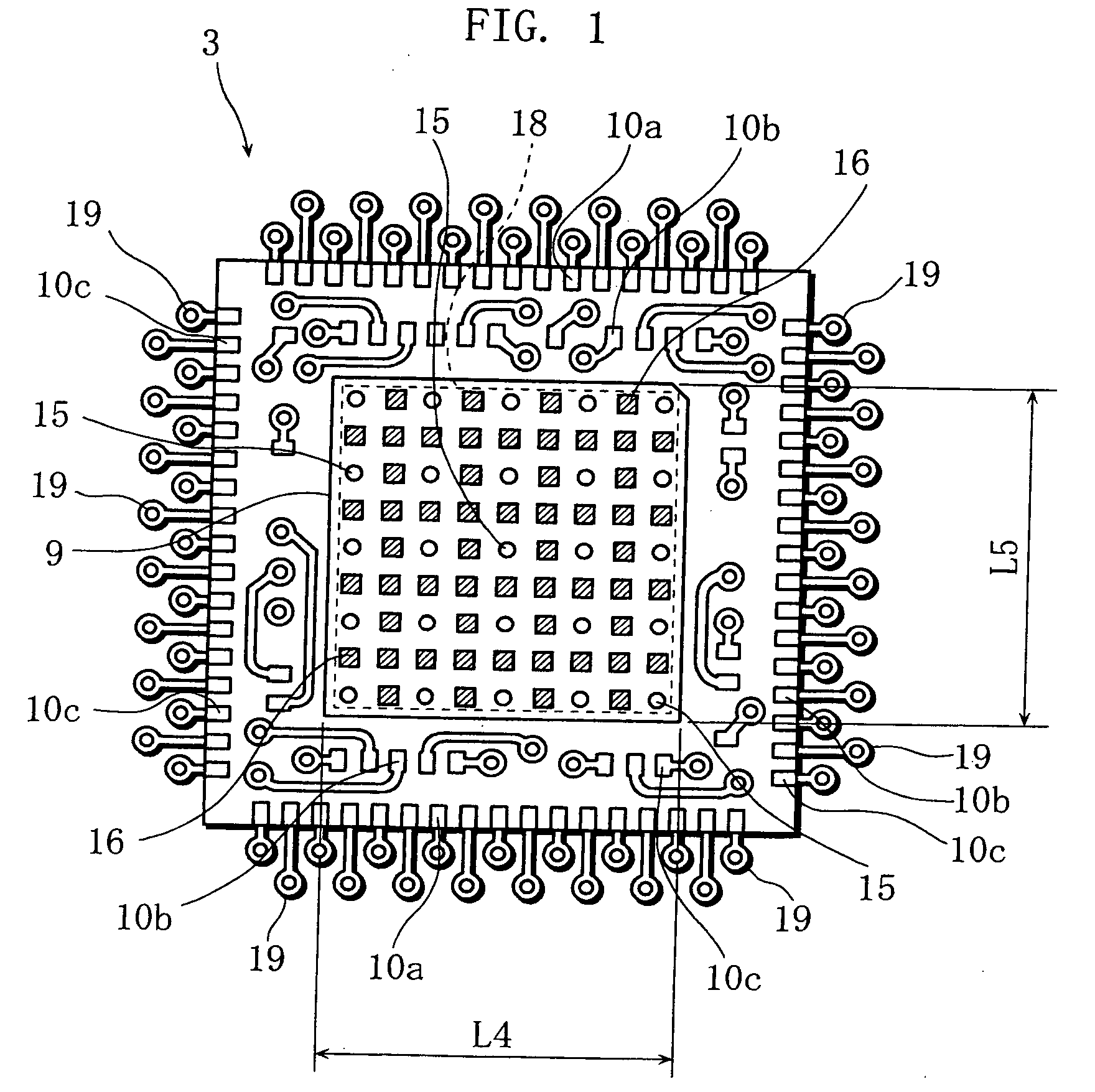
[0010] When the one or more gas-vent through holes passing through the package substrate are formed within the substrate-side center electrode, it is possible to prevent the semiconductor device from being elevated even if gas generation occurs during solder reflow, because the gas can be discharged outside through the one or more gas-vent through holes. Accordingly, the semiconductor device is prevented from being mounted inclined with respect to the package substrate. Therefore, it is possible to prevent the short circuits due to the solder paste being pressed between the device-side peripheral electrodes and the substrate-side peripheral electrodes and the disconnections due to the insufficiency of solder paste between the device-side peripheral electrodes and the substrate-side peripheral electrodes.
[0011] In addition, since the one or more gas-vent through holes are formed within the soldering region in the substrate-side center electrode, gas discharging is carried out more smoothly.
[0013] The above-described construction makes it possible to avoid the drawbacks of gas discharge hindrance caused by the solder paste being plugged into the one or more gas-vent through holes and of short circuits caused by the solder paste coming out to the back side through the one or more gas-vent through holes; therefore, the foregoing operations and effects can be exhibited more effectively.
[0015] When a plurality of gas-vent through holes are arranged within the soldering region uniformly, the gas generated in any location can be discharged outside through the gas-vent through holes smoothly. In addition, since there are a plurality of separate soldered portions, the surface tension in each of the soldered portion reduces. For these reasons, it is possible to more effectively prevent the semiconductor device from being elevated and to more effectively prevent the semiconductor device from being mounted inclined with respect to the package substrate.
[0016] Moreover, since the soldered portions are arranged so that their distribution density is uniform within the soldering region, the distances between the soldered portions become short. Therefore, stabilization of the ground potential is achieved, making it possible to maintain good high-frequency performance.
[0022] With the above-described construction, the pressure applied to each solder paste becomes uniform when the semiconductor device is placed on the solder paste, making it possible to prevent the semiconductor device from being mounted inclined with respect to the package substrate more effectively and exhibit the operations and effects further.

Problems solved by technology

A problem with the above-described conventional construction, however, is that disconnections and short circuits occur at power supply electrodes or the like formed in the periphery of the ground electrode.
Consequently, such problems arise that short circuits occur because the solder paste is pressed between the device-side power supply electrode 52a and the substrate-side power supply electrode 55a and that disconnections occur between the device-side power supply electrode 52b and the substrate-side power supply electrode 55b due to an insufficiency of the solder paste.

Method used


Image

  • Land grid array package
  • Land grid array package
  • Land grid array package

Examples


example 1

[0042] The above-described land grid array package according to the best mode for carrying out the invention was employed as Example 1.

[0043] The land grid array package thus fabricated is hereafter referred to as Package A of the invention.

example 2

[0044] A land grid array package was fabricated in the same manner as in Example 1 above except that solder paste 25 was applied forming four separate squared shapes as illustrated in FIG. 5.

[0045] The land grid array package thus fabricated is hereafter referred to as Package B of the invention.

[0046] It should be noted that, in FIG. 5, mentioned above, and FIGS. 6 to 9, which will be referred to later, the leads of the outlet terminals 19 are omitted for simplicity in illustration.

example 3

[0047] A land grid array package was fabricated in the same manner as in Example 1 above except that solder paste 25 was applied forming three separate regions as illustrated in FIG. 6.

[0048] The land grid array package thus fabricated is hereafter referred to as Package C of the invention.


PUM


Abstract

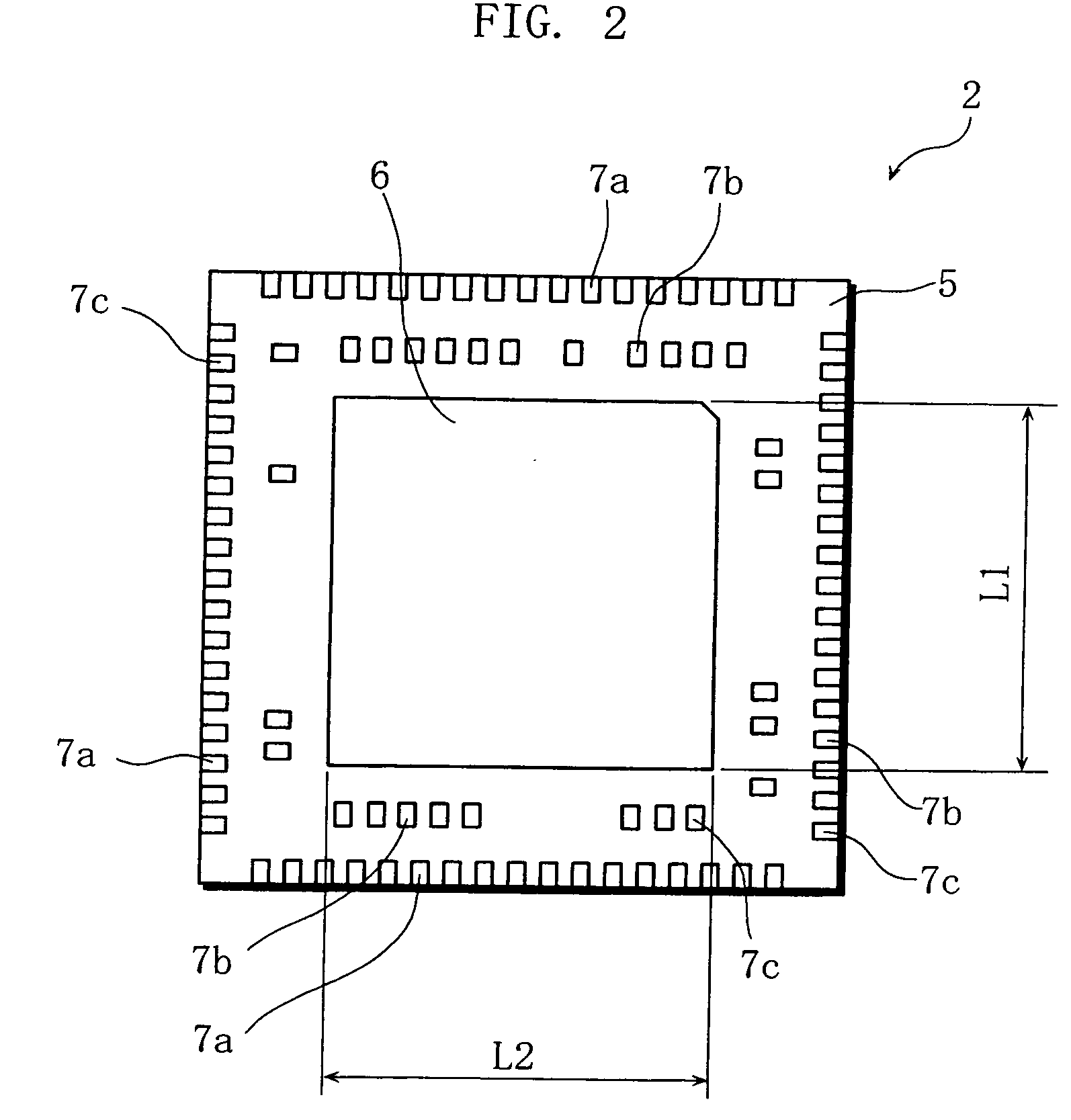
A land grid array package has a construction in which a device-side ground electrode 6 and a substrate-side ground electrode 9, as well as device-side peripheral electrodes 7 and substrate-side peripheral electrodes 10 are soldered by eutectic solder 16. The land grid array package is characterized in that one or more gas-vent through holes 15 passing through a package substrate 3 are formed within a soldering region 18 of the device-side ground electrode 6. Thus, a land grid array package that can prevent short circuits or disconnections is provided.

Description

TECHNICAL FIELD [0001] The present invention relates to land grid array packages, and more particularly to land grid array packages used for wireless communication modules. BACKGROUND ART [0002] Recently, in order to increase packaging density and achieve size reduction etc. of electronic devices, new forms of semiconductor packages have been proposed such as ball grid arrays and land grid arrays, which are leadless packages and in which contact electrodes are made in grid form on back faces of the packages. In particular, those of the land grid array type are often used for high-frequency ICs or high-power ICs. [0003] The high-frequency ICs have such a construction in which a large-area ground electrode (die pad) is formed in a central region of the back side of the package and the entire ground electrode is subjected to soldering. Such a construction is employed for the purpose of stabilizing ground potential and maintaining good high-frequency performance by soldering (or making ...

Claims


Application Information

Patent Timeline
IPC IPC(8): H01L23/48H01L23/52H01L29/40H01L23/12H05K3/34
CPCH05K3/341H05K2201/09063H05K2201/09663H05K2201/10727H05K2201/10969H05K2203/1178H01L2224/73257H01L24/73H01L2224/48091H01L2924/00014H01L2924/01322Y02P70/50H01L2924/00
Inventor SUZUKA, TAKUYA
Owner SANYO ELECTRIC CO LTD
Learn More