

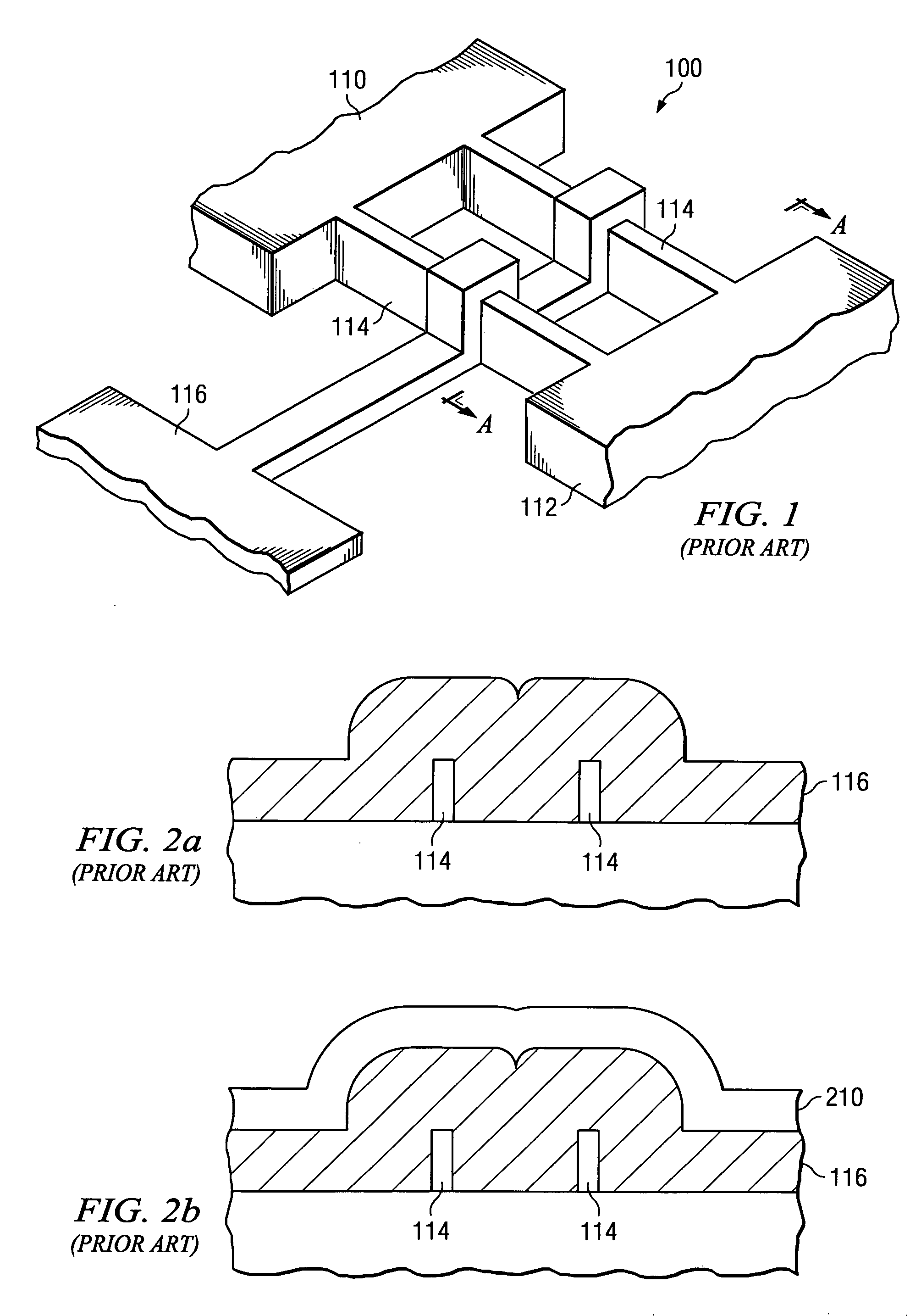
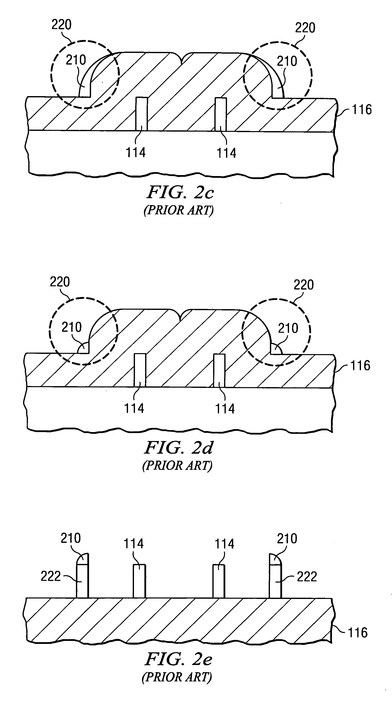
Trench-gate electrode for FinFET device
- Summary
- Abstract
- Description
- Claims
- Application Information
AI Technical Summary
Benefits of technology
Problems solved by technology
Method used
Image

Examples
Embodiment Construction
[0023] The making and using of the presently preferred embodiments are discussed in detail below. It should be appreciated, however, that the present invention provides many applicable inventive concepts that can be embodied in a wide variety of specific contexts. The specific embodiments discussed are merely illustrative of specific ways to make and use the invention, and do not limit the scope of the invention.
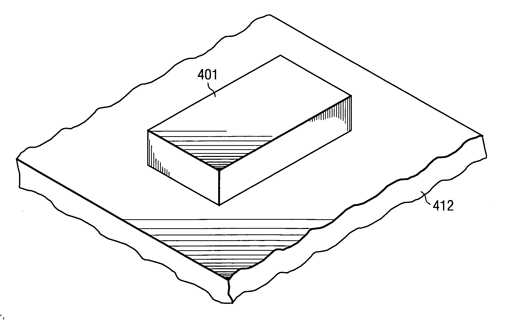
[0024] The present invention will be described in the context of a dual-fin FinFET. Embodiments of the present invention, however, may be used in a variety of contexts. For example, embodiments of the present invention may be used to fabricate FinFETs having fewer or more fins or any other type of device in which the topography is such that it is difficult to completely remove unwanted mask material. Furthermore, embodiments of the present invention have been found to be particularly useful when using 193 nm and below lithography techniques.
[0025] It should be noted that e...
PUM
 Abstract
Description
Claims
Application Information