Strained channel complementary field-effect transistors and methods of manufacture

a complementary field-effect transistor and strain-coupling technology, which is applied in the direction of basic electric elements, semiconductor devices, electrical equipment, etc., can solve the problems of high defect density of substrates, high cost of approach, and strain-relaxation

Inactive Publication Date: 2006-08-24
TAIWAN SEMICON MFG CO LTD
View PDF99 Cites 91 Cited by
  • Summary
  • Abstract
  • Description
  • Claims
  • Application Information

AI Technical Summary

Benefits of technology

[0010] In prior art schemes of inducing strain in transistors, the introduction of a strain by a stressor may benefit transistors of the first conduction type while degrading transistors of the second conduction type. This and other problems are generally solved or circumvented, and technical advantages are generally achieved, by preferred embodiments of the present invention, which provide a method of manufacturing strained n-channel and p-channel field effect transistors with separately optimized performance.

Problems solved by technology

But there are concerns about the strain relaxation upon subsequent CMOS processing where high temperatures are used.
In addition, this approach is very expensive since a SiGe buffer layer with thickness in the order of micrometers has to be grown.
Numerous dislocations in the relaxed SiGe buffer layer exist and some of these dislocations propagate to the strained silicon layer, resulting in a substrate with high defect density.
Thus, this approach has limitations that are related to cost and fundamental material properties.
However, uniaxial tensile strain degrades the hole mobility while uniaxial compressive strain degrades the electron mobility.
Ion implantation of germanium can be used to selectively relax the strain so that the hole or electron mobility is not degraded, but this is difficult to implement due to the close proximity of the n and p-channel transistors.

Method used


Image

  • Strained channel complementary field-effect transistors and methods of manufacture
  • Strained channel complementary field-effect transistors and methods of manufacture
  • Strained channel complementary field-effect transistors and methods of manufacture

Examples


Embodiment Construction

[0020] The making and using of the presently preferred embodiments are discussed in detail below. It should be appreciated, however, that the present invention provides many applicable inventive concepts that can be embodied in a wide variety of specific contexts. The specific embodiments discussed are merely illustrative of specific ways to make and use the invention, and do not limit the scope of the invention.

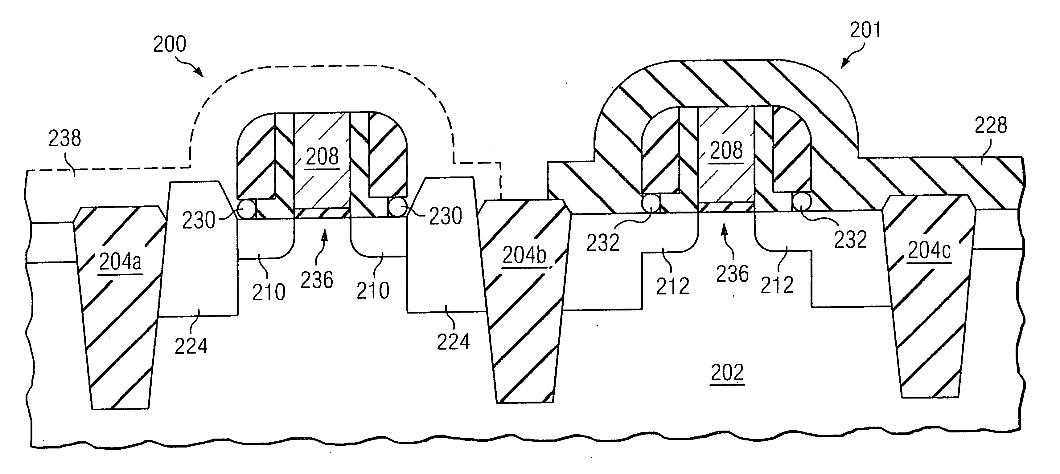
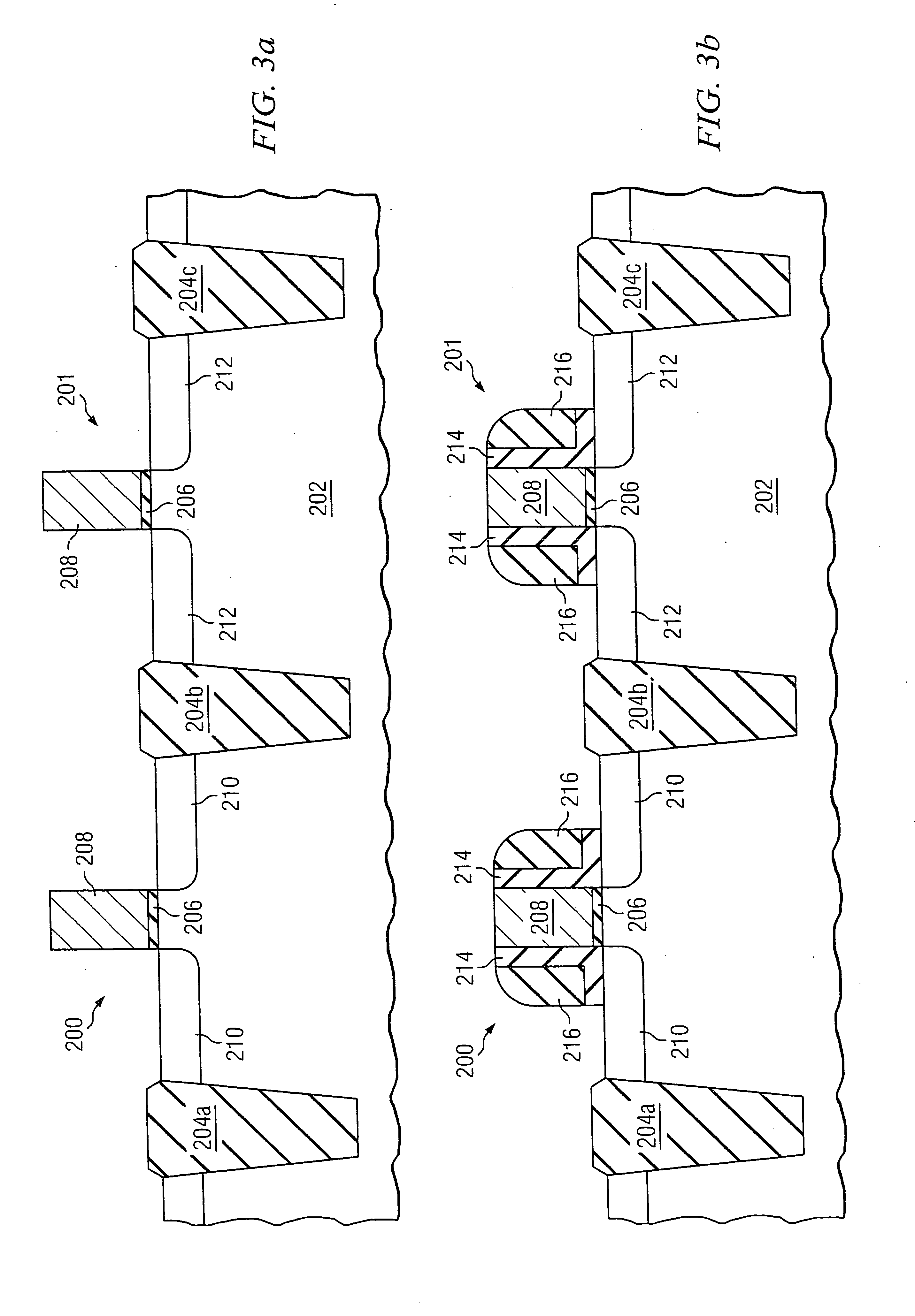
[0021] The preferred embodiment of the present invention relates to the field of semiconductor devices, and more specifically, to the manufacture of strained n-channel and p-channel field effect transistors with separately optimized performance.

[0022] With the preferred embodiment it is possible to separately optimize the performance of n-channel and p-channel transistors by engineering the nature and magnitude of the strain in the channel region of the transistors. For example, it is desirable to induce a tensile strain in the channel of the n-channel transistor in the so...


PUM


Abstract

A transistor includes a gate dielectric overlying a channel region. A source region and a drain region are located on opposing sides of the channel region. The channel region is formed from a first semiconductor material and the source and drain regions are formed from a second semiconductor material. A gate electrode overlies the gate dielectric. A pair of spacers is formed on sidewalls of the gate electrode. Each of the spacers includes a void adjacent the channel region. A high-stress film can overlie the gate electrode and spacers.

Description

[0001] This application is a divisional of patent application Ser. No. 10 / 639,170 (TSM03-0467), entitled “Strained Channel Complementary Field-Effect Transistors and Methods of Manufacture,” filed Aug. 12, 2003, which application is incorporated herein by reference. CROSS-REFERENCE TO RELATED APPLICATIONS [0002] This application relates to co-pending and commonly assigned patent application Ser. No. 10 / 423,513 (TSM03-0173), filed Apr. 25, 2003, entitled “Strained Channel Transistor and Methods of Manufacture,” and Ser. No. 10 / 379,033 filed Feb. 28, 2003, (TSM03-0050) entitled “Strained-channel transistor with a lattice-mismatched zone in the source / drain regions.” Both applications are hereby incorporated herein by reference.TECHNICAL FIELD [0003] The present invention relates generally to semiconductor devices, and more particularly, the preferred embodiment relates to strained channel complementary field-effect transistors and methods of manufacture. BACKGROUND [0004] Size reducti...

Claims


Application Information

Patent Timeline
Patent Type & Authority Applications(United States)
IPC IPC(8): H01L21/8234H01L21/8238
CPCH01L21/823807H01L21/823814H01L21/823864H01L29/66636H01L29/7843H01L29/7848
Inventor KO, CHIH-HSINYEO, YEE-CHIALEE, WEN-CHINHU, CHENMING
Owner TAIWAN SEMICON MFG CO LTD
Why Eureka
Try Eureka