10t nvsram cell and cell operations

a technology of nvsram and nvsram memory, applied in the field of 10 t nvsram cell and cell operation, can solve the problem of large 12t cell size of nmos nvsram memory, and achieve the effect of high array efficiency

Inactive Publication Date: 2014-04-24
APLUS FLASH TECH
View PDF6 Cites 11 Cited by
  • Summary
  • Abstract
  • Description
  • Claims
  • Application Information

AI Technical Summary

Benefits of technology

[0033]In yet still another alternative embodiment, the present invention provides a method for setting initial power lines of each 6T SRAM cell to VDDP and VSSP in a reversed manner for cancelling the mismatches of the paired NMOS devices in each SRAM cell without consuming any DC standby current. The reversed initial setup means setting VDDP to VSS but VSSP to VDD. Note that the NW nodes of both Inverters of the SRAM cell are kept at VDD.
[0037]As a result, the traditional 12T NVSRAM cell would be reduced to only 10 transistors. Because each Select transistor is a HV device with larger channel length, the cell size saving of NVSRAM is more than the simple ratio of 10 / 12. In addition to the space saved from removing two HV bottom Select transistors, a common sourceline of each paired Flash strings can be also removed from each flash cell to leave source node floating if a DRAM-like charge-sensing scheme is used for SRAM Recall operation. Alternatively, the Store operation of the 10T NVSRAM cell can be operated by using a current-charging scheme from a shared Fpower line to draw VDD power to send current to charge the paired Q and QB nodes of each 6T SRAM cell through the paired Flash cell acted as Voltage Follower that stored ΔVtp≧1.0V. Each SRAM's amplification is preferably divided into a 2-step approach by first ramping down SRAM power line VSSP from the VDD level to VSS=0V, and conversely ramping up SRAM power line VDDP from VSS to the VDD level. After this 2-step SRAM amplification process, the Q and QB node voltage difference of about 0.4V can be fully amplified to VDD and VSS digital levels to define standard SRAM logic state. In addition, the FN-channel erase, FN-channel program and FN-edge program schemes can be flexibly used for operating these 10T NVSRAM cell at VDD operation as low as 1.2V without need of SBPI method, thus no top and bottom Select transistors are really required. The final effective area saving in this 10T NVSRAM cell size is about 25% compared to the conventional 12T NVSRAM cell size. For today's NVSRAM design with a demand for density higher than 4 Mb, the die size saving is more than 20% because a typical NVSRAM cell array takes up more than 80% of the total final die size due to high array efficiency.

Problems solved by technology

One big drawback of this 12T NMOS NVSRAM memory is its large 12T cell size that comprises one 6T LV SRAM cell and one 6T HV Flash cell.

Method used


Image

  • 10t nvsram cell and cell operations
  • 10t nvsram cell and cell operations
  • 10t nvsram cell and cell operations

Examples


Embodiment Construction

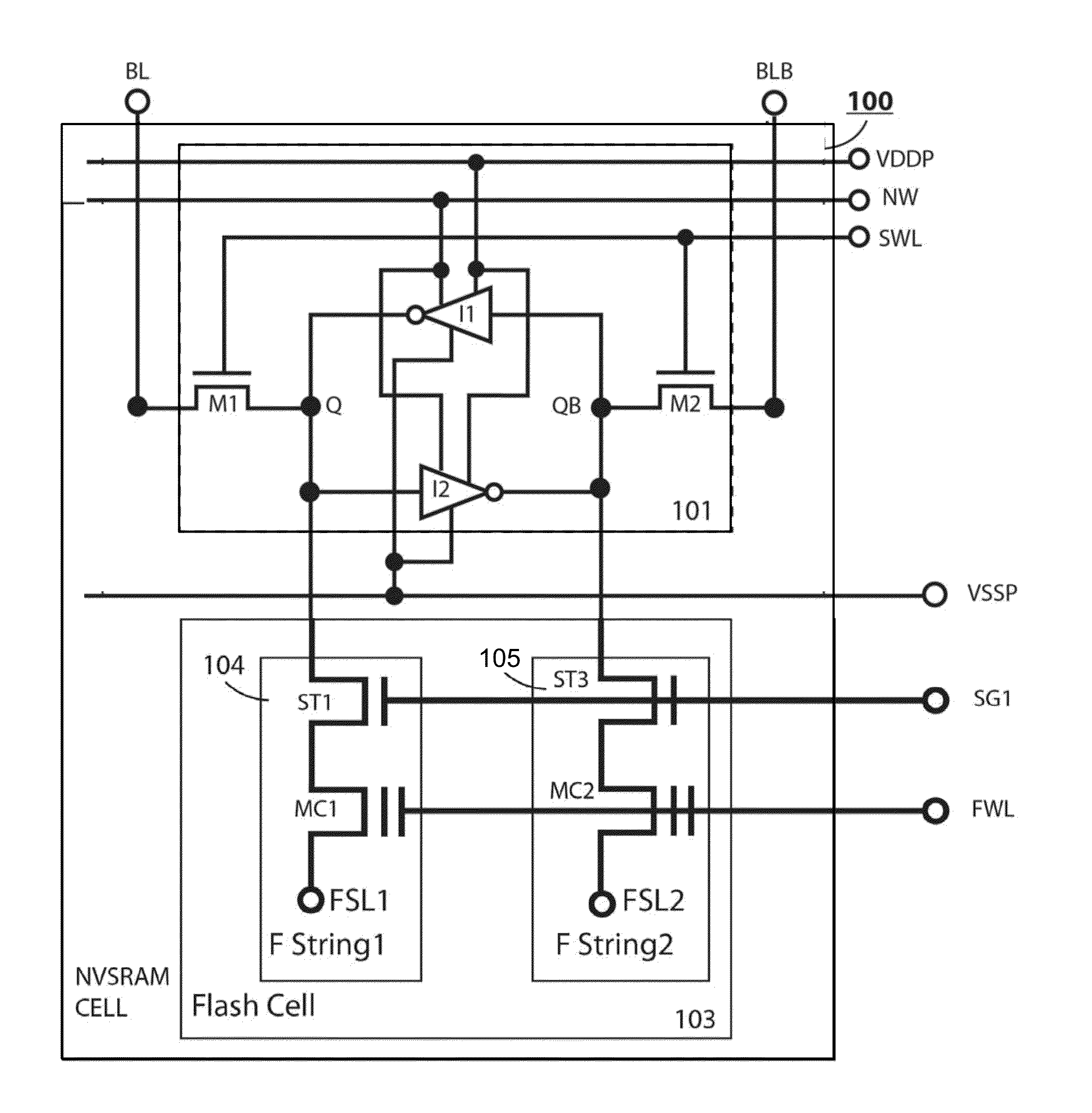
[0051]The present invention is related to improvement in NVSRAM cell size over the traditional 12T NVSRAM cell by using fewer transistors, becoming a 10T NVSRAM cell. The 10T NVSRAM cell can be configured to in several biased conditions for successful NVSRAM operation. The same cell-size reduction improvement can be applied to those all NVSRAM cells that comprises at least one paired 3T Flash strings, regardless of flash type made of NMOS or PMOS, regardless of 2-poly Floating-gate or 1-poly Charge-trapping SONOS or MONOS devices. A preferred 10T NVSRAM cell is provided by removing one bottom HV Select transistor from each 3T Flash string. Thus one paired Flash strong would save two HV Select transistors.

[0052]In a specific embodiment, the 10T NVSRAM cell circuit can be configured by removing one paired HV bottom Select transistors from the traditional 12T NVSRAM cell that comprises one 6T LV SRAM cell and one HV flash cell that further comprises one paired 3T flash FStrings. Each 3...


PUM


Abstract

A 10T NVSRAM cell is provided with a bottom HV NMOS Select transistor in each 3T FString removed from traditional 12T NVSRAM cell. A Recall operation by reading a stored ΔVt state of flash transistors into each SRAM cell uses a charge-sensing scheme rather than the current-sensing scheme, with all other key operations unchanged. The Recall operation works under any ramping rate of SRAM's power line voltage and Flash gate signal which can be set higher than only Vt0 or both Vt0 and Vt1. Alternatively, the Store operation can use a current charging scheme from a Fpower line to the paired Q and QB nodes of each SRAM cell through a paired Flash Voltage Follower that stored ΔVtp≧1.0V. The Recall operation in this alternative embodiment is to use a 7-step approach with the FN-channel erase, FN-channel program and FN-edge program schemes, including 2-step SRAM amplification.

Description

CROSS-REFERENCE TO RELATED APPLICATIONS[0001]This application claims priority to U.S. Patent Application No. 61 / 716,415, filed on Oct. 19, 2012, and also claims priority to U.S. Patent Application No. 61 / 723,270, filed on Nov. 6, 2012, commonly assigned, and hereby incorporated by references in their entireties herein for all purposes.[0002]This application is related to U.S. Pat. No. 7,164,608, U.S. patent application Ser. No. 14 / 037,356, U.S. Provisional Application Nos. 61 / 714,186, 61 / 719,344, and 61 / 720,385, commonly assigned, which are incorporated by reference herein for all purposes.[0003]Additionally, this application is related to U.S. Pat. Nos. 5,065,362 and 7,760,540.TECHNICAL FIELD OF THE INVENTION[0004]The present embodiments relate to an improvement in NVSRAM cell size over the traditional NVSRAM cell by using fewer transistors. Merely by example, a 10T NVSRAM cell is provided with one LV 6T SRAM cell and one HV 4T Flash cell that further comprises one paired fully sym...

Claims


Application Information

Patent Timeline
Patent Type & Authority Applications(United States)
IPC IPC(8): G11C14/00
CPCG11C14/0063
Inventor TSAO, HSING-YALEE, PETER WUNG
Owner APLUS FLASH TECH
Why Eureka
Try Eureka