Reconfigurable processor module comprising hybrid stacked integrated circuit die elements

a processor module and integrated circuit technology, applied in the field of reconfigurable data processing systems and methods, can solve the problems of requiring millions of processor clock cycles in order to complete reconfiguration, and the application space over which such reconfigurable processors can be practically employed, and achieve the effect of reducing the test time of dies

Inactive Publication Date: 2006-08-31
ARBOR GLOBAL STRATEGIES LLC
View PDF11 Cites 316 Cited by
  • Summary
  • Abstract
  • Description
  • Claims
  • Application Information

AI Technical Summary

Benefits of technology

[0009] In accordance with the disclosure of a representative embodiment of the present invention, FPGAs, microprocessors and cache memory may be combined through the use of recently available wafer processing techniques to create a particularly advantageous form of hybrid, reconfigurable processor module that overcomes the limitations of present discrete, integrated circuit device implementations of GPRP systems. As disclosed herein, this new processor module may be conveniently denominated as a Stacked Die Hybrid (“SDH”) Processor.
[0010] Tru-Si Technologies of Sunnyvale, Calif. (http: / / www.trusi.com) has developed a process wherein semiconductor wafers may be thinned to a point where metal contacts can traverse the thickness of the wafer creating small bumps on the back side much like those of a BGA package. By using a technique of this type in the manufacture of microprocessor, cache memory and FPGA wafers, all three die, or combinations of two or more of them, may be advantageously assembled into a single very compact structure thus eliminating or ameliorating each of the enumerated known difficulties encountered with existing reconfigurable technology discussed above.
[0011] Moreover, since these differing die do not require wire bonding to interconnect, it is now also possible to place interconnect pads throughout the total area of the various die rather than just around their periphery. This then allows for many more connections between the die than could be achieved with any other known technique.

Problems solved by technology

In practice however, the application space over which such reconfigurable processors, (as well as hybrids combining both microprocessors and FPGAs) can be practically employed is limited by several factors.
Firstly, since FPGAs are less dense than microprocessors in terms of gate count, those packaged FPGAs having sufficient gates and pins to be employed as a general purpose reconfigurable processor (“GPRP”), are of necessity very large devices.
This size factor alone may essentially prohibit their use in many portable applications.
Secondly, the time required to actually reconfigure the chips is on the order of many hundreds of milliseconds, and when used in conjunction with current microprocessor technologies, this amounts to a requirement of millions of processor clock cycles in order to complete the reconfiguration.
This again limits its usefulness to applications that require the job not be context-switched.
For the GPRP this would mean it would have to again reconfigure itself thereby wasting even more time.
Thirdly, since microprocessors derive much of their effective operational speed by operating on data in their cache, transferring a portion of a particular job to an attached GPRP would require moving data from the cache over the microprocessor's front side bus to the FPGA.
Since this bus runs at about 25% of the cache bus speed, significant time is then consumed in moving data.
This again effectively limits the reconfigurable processor to applications that have their data stored elsewhere in the system.
As a result, the throughput benefits that reconfigurable computing can offer to a hybrid system made up of existing, discrete microprocessors and FPGAs may be obviated or otherwise limited in its potential usefulness.

Method used


Image

  • Reconfigurable processor module comprising hybrid stacked integrated circuit die elements
  • Reconfigurable processor module comprising hybrid stacked integrated circuit die elements
  • Reconfigurable processor module comprising hybrid stacked integrated circuit die elements

Examples


Embodiment Construction

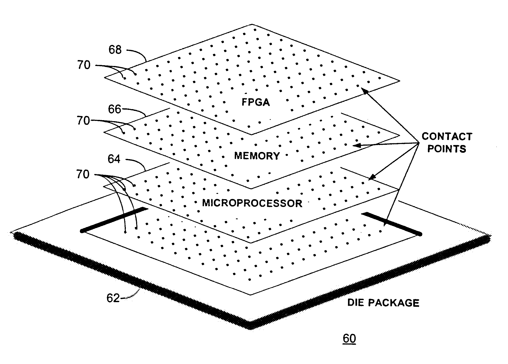
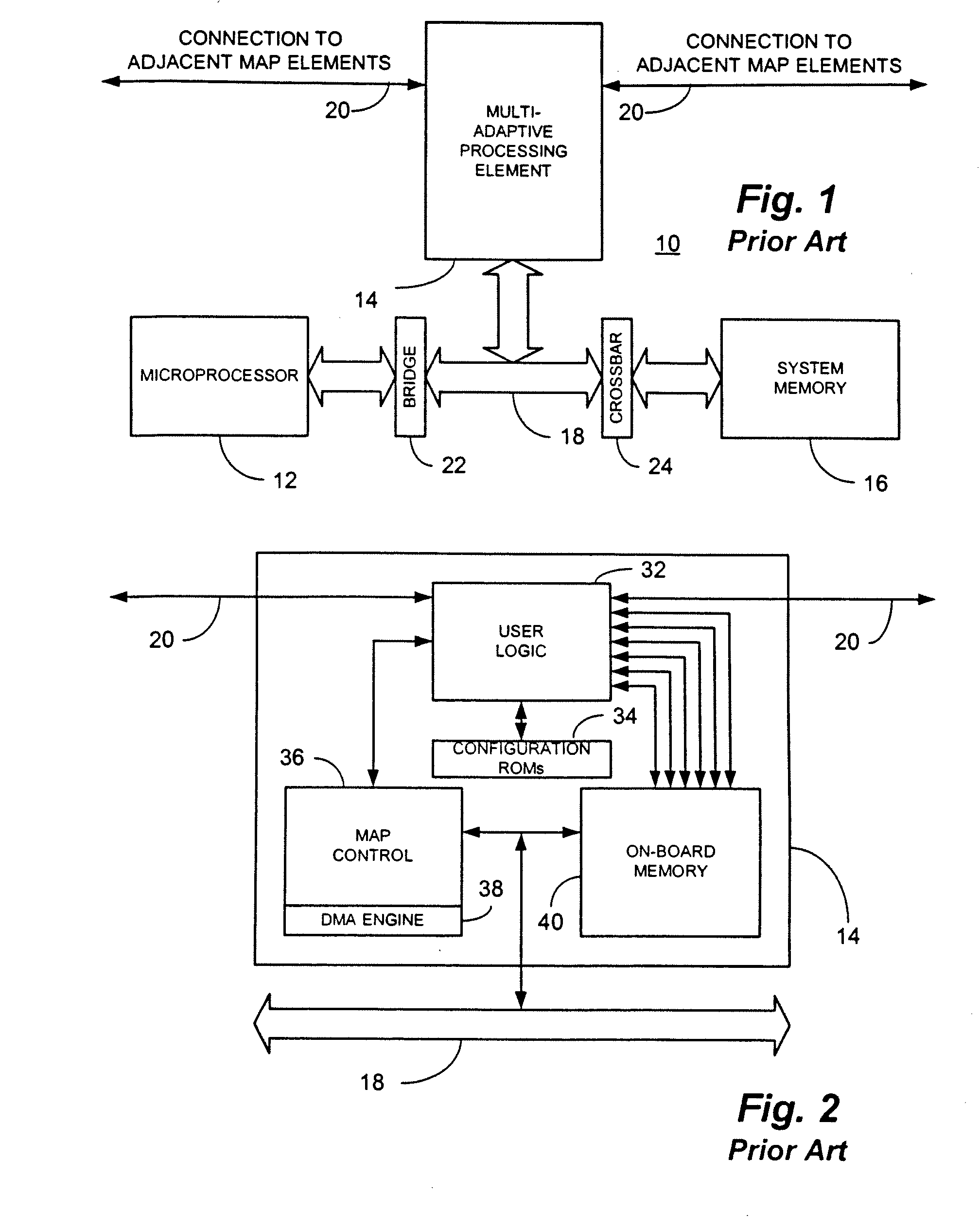
[0028] With reference now to FIG. 1, a simplified functional block diagram of a portion of a prior art reconfigurable computer system 10 is shown. The computer system 10 incorporates, in pertinent part, one or more microprocessors 12, one or more multi-adaptive processing (MAP™) elements 14 and an associated system memory 16. A system bus 18 bidirectionally couples a MAP element 14 to the microprocessor 12 by means of a bridge 22 as well as to the system memory 16 by means of a crossbar switch 24. Each MAP element 14 may also include one or more bidirectional connections 20 to other adjacent MAP elements 14 as shown

[0029] With reference additionally now to FIG. 2, a more detailed, simplified functional block diagram of the multi-adaptive processing element 14 illustrated in the preceding figure is shown. The multi-adaptive processing element 14 comprises, in pertinent part, a user logic block 32, which may comprise an FPGA together with its associated configuration ROM 34. A MAP co...


PUM


Abstract

A reconfigurable processor module comprising hybrid stacked integrated circuit (“IC”) die elements. In a particular embodiment disclosed herein, a processor module with reconfigurable capability may be constructed by stacking one or more thinned microprocessor, memory and / or field programmable gate array (“FPGA”) die elements and interconnecting the same utilizing contacts that traverse the thickness of the die. The processor module disclosed allows for a significant acceleration in the sharing of data between the microprocessor and the FPGA element while advantageously increasing final assembly yield and concomitantly reducing final assembly cost.

Description

RELATED APPLICATION [0001] The present application is a Continuation of U.S. patent application Ser. No. 10 / 802,067 filed Mar. 16, 2004 which is a Continuation-In-Part of U.S. patent application Ser. No. 10 / 452,113, now issued U.S. Pat. No. 6,781,226 filed Jun. 2, 2003, which is a Continuation of U.S. patent application Ser. No. 10 / 012,057, now issued U.S. Pat. No. 6,627,985 filed Dec. 5, 2001, all of which are incorporated herein by reference in their entirety and are assigned to the assignee of the present application.BACKGROUND OF THE INVENTION [0002] The present invention relates, in general, to the field of systems and methods for reconfigurable, or adaptive, data processing. More particularly, the present invention relates to an extremely compact reconfigurable processor module comprising hybrid stacked integrated circuit (“IC”) die elements. [0003] In addition to current commodity IC microprocessors, another type of processing element is commonly referred to as a reconfigurab...

Claims


Application Information

Patent Timeline
Patent Type & Authority Applications(United States)
IPC IPC(8): G06F11/00G06F15/78H01L21/98H01L25/065H01L25/18
CPCG06F15/7867H01L23/481H01L25/0657H01L25/18H01L25/50H01L2225/06513Y02B60/1225H01L2225/06524H01L2224/05H01L2224/0401H01L2224/04042Y02B60/1207H01L2225/06517Y02D10/00
Inventor HUPPENTHAL, JON M.GUZY, D. JAMES
Owner ARBOR GLOBAL STRATEGIES LLC
Why Eureka
Try Eureka