Organic electroluminescent device, pixel structure, array and driving method thereof

Active Publication Date: 2006-09-07
III HLDG 1
View PDF6 Cites 12 Cited by
  • Summary
  • Abstract
  • Description
  • Claims
  • Application Information

AI Technical Summary

Benefits of technology

[0010] Accordingly, the present invention is directed to provide an organic electroluminescent device and p

Problems solved by technology

However, there are uncertain factors in the process with possibly a decrease in process re

Method used


Image

  • Organic electroluminescent device, pixel structure, array and driving method thereof
  • Organic electroluminescent device, pixel structure, array and driving method thereof
  • Organic electroluminescent device, pixel structure, array and driving method thereof

Examples


Embodiment Construction

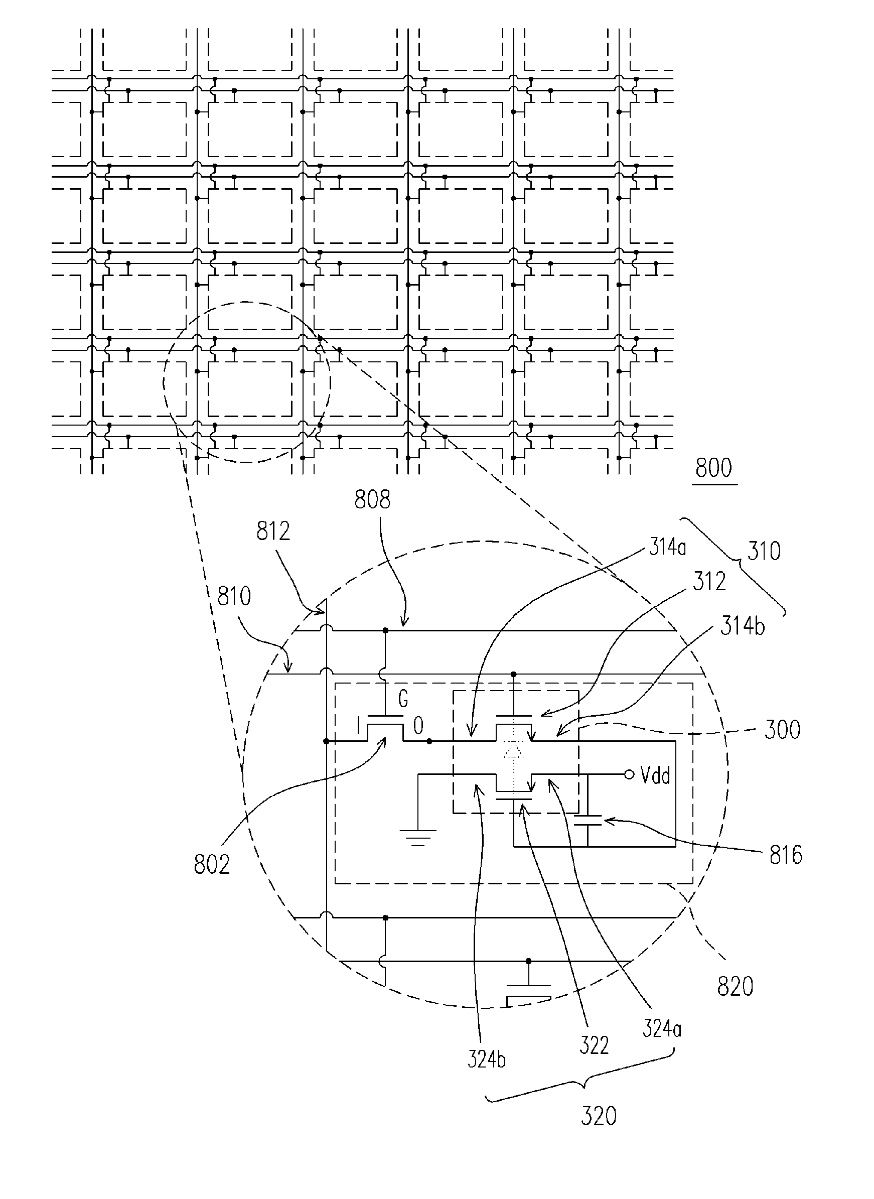
[0033] Using the gates of the organic thin film transistor as the top electrode and the bottom electrode of the organic electroluminescent device, the present invention widens the aperture ratio of the organic electroluminescent device. The present invention will be explained below with reference to exemplary embodiments thereof, it will be understood by those of ordinary skill in the art that these embodiments are not used for limiting the present invention and various changes in form and details may be made therein without departing from the spirit and scope of the present invention as defined by the following claims.

[0034]FIG. 3 is a stereogram of an organic electroluminescent device according to an exemplary embodiment of the present invention. Referring to FIG. 3, the organic electroluminescent device 300 includes a first organic thin film transistor 310, a second organic thin film transistor 320, and at least one organic functional layer 330. The first organic thin film trans...


PUM


Abstract

An organic electroluminescent device includes a first organic thin film transistor, a second organic thin film transistor and at least an organic functional layer. The organic functional layer is disposed between the second organic thin film transistor and the first organic thin film transistor. By applying voltages in the first organic thin film transistor and the second organic thin film transistor at the same time, a voltage difference between the two transistors is produced to make electrons and electric holes move into the organic functional layer and re-combine therein for emitting light. The integration of the organic thin film transistor and the organic electroluminescent device can widen aperture ratio and increase process reliability.

Description

CROSS-REFERENCE TO RELATED APPLICATION [0001] This application claims the priority benefit of Taiwan application serial no. 93137589, filed on Dec. 6, 2004. All disclosure of the Taiwan application is incorporated herein by reference. BACKGROUND OF THE INVENTION [0002] 1. Field of Invention [0003] The present invention relates to a light-emitting device, and more particularly, to an organic electroluminescent (OEL) device and pixel structure, array and driving method thereof. [0004] 2. Description of Related Art [0005] Along with the advancement of multimedia information communication technology, the importance of displays in providing human the access to computer interface has increasingly acknowledged. The flat panel display (FPD) has become the mainstream product in the market because of high-quality resolution, efficient space utilization, low power consumption, and the freedom of radiation exposure. [0006] The so-called flat panel displays include liquid crystal displays (LCD),...

Claims


Application Information

Patent Timeline
IPC IPC(8): G09G3/10H01L29/08H01L35/24
CPCG09G3/3233G09G2300/0465G09G2300/0842G09G2310/0262H01L27/283H01L27/3274H10K19/10H10K59/125
Inventor LIN, EN-CHIANGLIAO, CHI-CHIH
Owner III HLDG 1
Why Eureka
Try Eureka