Photoresist removing method

A technology of photoresist and photoresist layer, which is applied in the direction of electrical components, semiconductor/solid-state device manufacturing, circuits, etc., and can solve problems such as low process reliability

Active Publication Date: 2013-06-05
SEMICON MFG INT (SHANGHAI) CORP
View PDF4 Cites 12 Cited by
  • Summary
  • Abstract
  • Description
  • Claims
  • Application Information

AI Technical Summary

Problems solved by technology

[0013] The object of the present invention is to provide a photoresist removal method to solve the problem

Method used


Image

  • Photoresist removing method
  • Photoresist removing method
  • Photoresist removing method

Examples


Embodiment Construction

[0027] The method for removing photoresist proposed by the present invention will be further described in detail below with reference to the accompanying drawings and specific embodiments. Advantages and features of the present invention will be apparent from the following description and claims. It should be noted that all the drawings are in a very simplified form and use imprecise scales, and are only used to facilitate and clearly assist the purpose of illustrating the embodiments of the present invention.
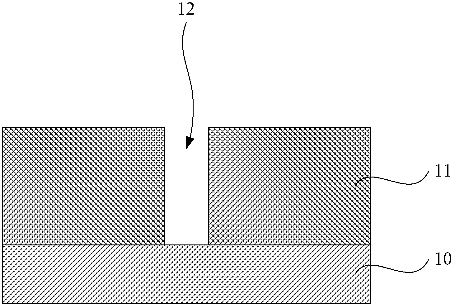
[0028] The core idea of ​​the present invention is to provide a photoresist removal method, which uses an oxygen-containing gas to perform a first ashing process on the photoresist layer to remove part of the photoresist layer; The resist layer is subjected to a second ashing process to remove the remaining photoresist layer. Since the second ashing process is performed on the remaining photoresist layer by using nitrogen-containing gas to remove the remaining photore...


PUM


Abstract

The invention provides a photoresist removing method which includes: performing a first ashing process on the photoresist layer through oxygen-containing gas to remove part of the photoresist layer; and performing a second ashing process on the remaining photoresist layer to remove the remaining photoresist layer. Due to the fact that the second ashing process is performed on the remaining photoresist layer through nitrogen-containing gas to remove the remaining photoresist, the problem that during manufacture of a magnetic random access memory (MEAM), when the photoresist is removed through a plasma of the oxygen-containing gas, the oxygen-containing gas can be reacted with a titanium nitride layer to form a titanium oxide layer on the surface of the titanium nitride layer, and a copper metal layer cannot be clearly observed when a process for forming a tunnel junction is performed is solved, and the reliability in forming the tunnel junction is improved.

Description

technical field [0001] The invention relates to an integrated circuit manufacturing process, in particular to a method for removing photoresist. Background technique [0002] MRAM (Magnetic Random Access Memory) is a non-volatile magnetic random access memory. It has the high-speed read and write capabilities of static random access memory (SRAM) and the high integration of dynamic random access memory (DRAM), and its power consumption is far lower than that of DRAM; compared with flash memory (Flash), MRAM It has the characteristic that the performance will not degrade with the increase of use time. Due to the above-mentioned characteristics of MRAM, it is called universal memory and is considered to be able to replace SRAM, DRAM, EEPROM and Flash. [0003] Unlike traditional random access memory chip fabrication technology, data in MRAM is not stored in the form of charge or current, but in a magnetic state, and is sensed by measuring resistance without disturbing the ma...

Claims


Application Information

Patent Timeline
IPC IPC(8): H01L21/027
Inventor 张海洋周俊卿
Owner SEMICON MFG INT (SHANGHAI) CORP
Why Eureka
Try Eureka