Liquid crystal display and method for driving same

a technology of liquid crystal display and display device, which is applied in the direction of static indicating device, non-linear optics, instruments, etc., can solve the problems of insufficient data signal applied to the pixel, complex fabrication of the additional color filter layer on the substrate, and insufficient light transmission for the color filter layer. achieve the effect of increasing the gate on time and improving the charging rate of the pixel electrod

Active Publication Date: 2006-09-07
SAMSUNG DISPLAY CO LTD
View PDF12 Cites 35 Cited by
  • Summary
  • Abstract
  • Description
  • Claims
  • Application Information

AI Technical Summary

Benefits of technology

[0012] Accordingly, it is an aspect of the present invention to provide an LCD improving a charging rate of the pixel electrode by increasing a gate on time and a driving method of the same.

Problems solved by technology

Further, fabricating the additional color filter layer on the substrate is intricate, and the transmittance of light for the color filter layer needs to be improved.
As the gate on time decreases, a data signal is not sufficiently applied to the pixel.
This causes a charging rate within the pixel electrode to be decreased and quality of the display apparatus to be deteriorated.

Method used


Image

  • Liquid crystal display and method for driving same
  • Liquid crystal display and method for driving same
  • Liquid crystal display and method for driving same

Examples


first embodiment

[0031] The first embodiment of the present invention will be appreciated by reference to FIGS. 1 and 2.

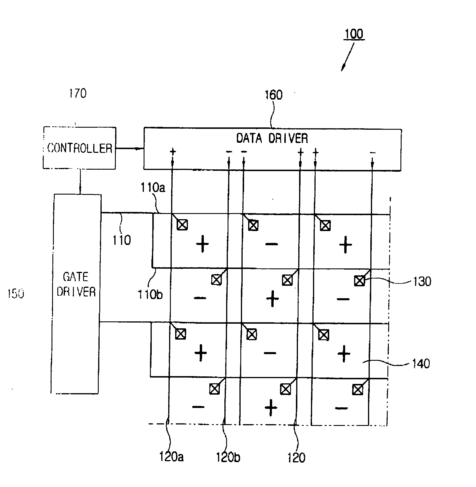
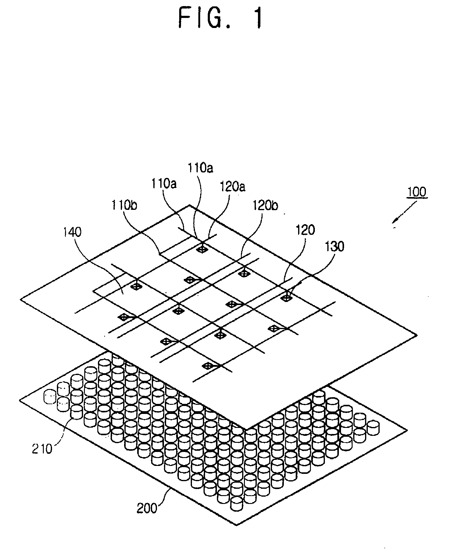
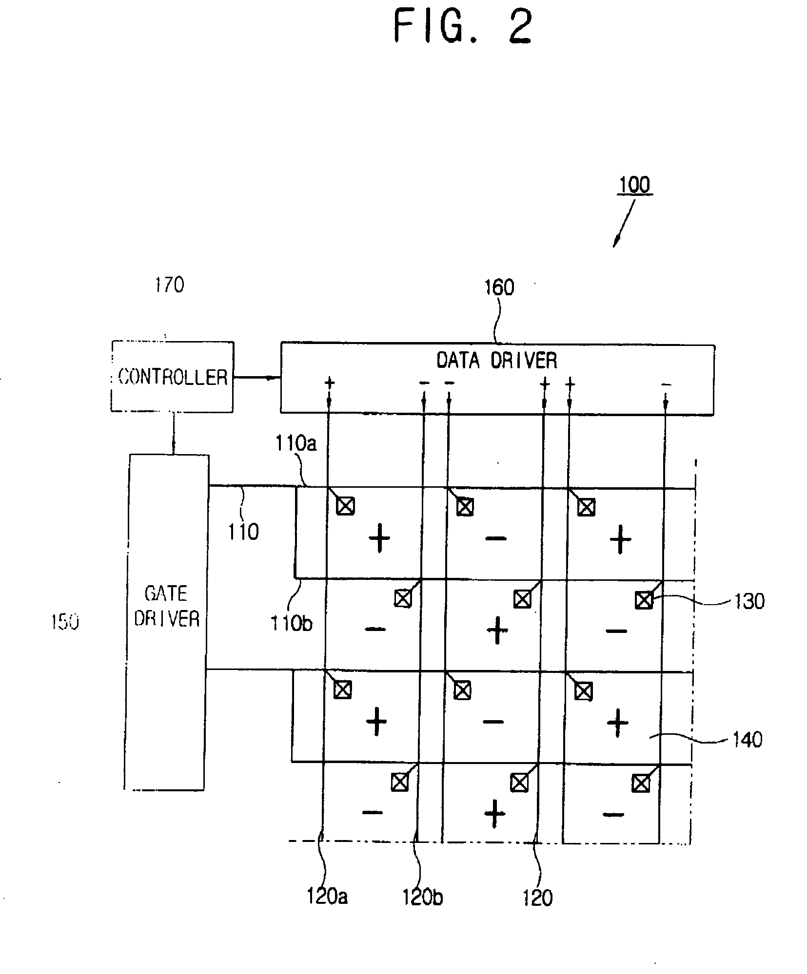
[0032] As shown in FIG. 1, an LCD comprises a TFT substrate 100 and an backlight unit 200.

[0033] The TFT substrate 100 comprises data lines 120, 120a and 120b; and gate lines 110a and 110b crossing the data lines 120a, 120b and 120 thereby forming a pixel area 140 arranged in a matrix array; and a TFT 130 disposed at an intersection of the gate line 110a and the data line 120.

[0034] Here, a pair of the gate lines 110a and 110b are connected with each other at their ends. Therefore, a single gate signal supplied by a gate driver (not shown) is applied to the pair of gate lines 110a and 110b at the same time. With this configuration, two rows of the pixel area 140 are driven for one gate on time.

[0035] In a conventional LCD, the gate signal supplied by a gate driver is applied to only one gate line at a time, thereby driving only one row of the pixel area 140. Unlike the conventi...

second embodiment

[0049] A second embodiment of a driving method of an LCD according to the present invention will be appreciated in by referring to FIG. 3 in connection with the following explanation.

[0050] The elements of the second embodiment that are identical to the elements of the first embodiment have the same reference numerals as the elements of the first embodiment. Moreover, the descriptions of the elements of the second embodiment that are identical to the elements of the first embodiment have been omitted for the sake of brevity. Data drive 160-1 differs from data drive 160 only in the order of the polarity of the output signals on the data lines.

[0051] As shown in FIG. 3, pixel areas 140 in a column direction are connected alternatively to the pair of data lines for data lines associated with the column of pixel areas. Adjacent columns of pixel areas 140 are symmetric with respect to the data line disposed therebetween. One of the adjacent pixel areas 140 in a row direction is connect...

third embodiment

[0053] Referring to FIG. 4, a driving method for an LCD according to a third embodiment of the present invention will be described. As shown in FIG. 4, gate lines 110c and 110d drive in common adjacent rows of pixels. For example, gate line 110c drives two rows of pixel areas 140a and 140b. Similarly, gate line 110d supplies a common gate signal to two rows of pixel areas 140c and 140d. Viewed in the column direction, the adjacent pixel areas 140a through 140d viewed from a data drive standpoint are electrically separated. Thus the adjacent pixel areas 140 in a column direction are supplied with different polarity data signals. Since gate line 110c drives the two rows of pixel area 140a and 140b, every TFT 130 belonging to the two rows of pixel areas 140a and 140b is connected to gate line 110c, and is connected to different rows of pixel areas 140 alternatively along the row direction. Controller 170 controls a data driver 160 so that adjacent pixel areas 140 viewed in the column d...


PUM

PropertyMeasurementUnit
frequencyaaaaaaaaaa
frequencyaaaaaaaaaa
areasaaaaaaaaaa

Abstract

Disclosed is an LCD comprising a plurality of data lines extending in a first direction, a plurality of gate lines extending in a second direction defining with the plurality of data lines a plurality of pixel areas arranged in a matrix configuration and supplying a gate signal to at least two rows of the pixel areas simultaneously. Thin film transistors are connected to the plurality of gate lines and the plurality of data lines. Also disclosed is a driving method for an LCD including a thin film transistor substrate including pixel areas arranged in a matrix form with a gate line extending in a first direction and a data line extending in a second direction, along with a backlight providing the TFT substrate with light of three primary colors. In the method, the three primary colors are sequentially provided in one frame period and at least two rows of pixel areas and simultaneously provided with a common gate signal.

Description

CROSS-REFERENCE TO RELATED APPLICATIONS [0001] This application claims the benefit of Korean Patent Application No. 2005-0017228, filed on Mar. 2, 2005, in the Korean Intellectual Property Office, the disclosure of which is incorporated herein by reference in its entirety. BACKGROUND OF THE INVENTION [0002] 1. Field of the Invention [0003] The present invention relates to a liquid crystal display (LCD) and a driving method of the same, and more particularly, to an LCD having an improved gate signal application and an improved gate signal application method. [0004] 2. Description of the Related Art [0005] Recently, there has been a desire for a lightweight and thin display apparatus. Such desire has caused CRTs (cathode ray tube) to be replaced with flat display apparatuses like an LCD. [0006] Typically an LCD display apparatus is comprised of two substrates and a liquid crystal layer having a dielectric anisotropy disposed therebetween. The LCD applies an electric field to the liqui...

Claims


Application Information

Patent Timeline
Patent Type & Authority Applications(United States)
IPC IPC(8): G02F1/136
CPCG02F1/136286G02F2001/133622G09G3/3413G09G3/3614G09G3/3648G09G2310/0205G09G2310/0235G09G2320/0223G02F1/133622G09G3/36G02F1/133
Inventor OH, JOO-HAKPARK, CHEOL-WOOCHAI, CHONG-CHUL
Owner SAMSUNG DISPLAY CO LTD
Why Eureka
Try Eureka