Semiconductor package fabrication

a semiconductor and package technology, applied in the manufacture of printed circuits, circuit inspection/indentification, basic electric elements, etc., can solve the problems of significant chemistry and waste produced, and the search has not revealed the drop on demand deposition used for fabricating the semiconductor package componen

Active Publication Date: 2006-09-14
INFINEON TECH AMERICAS CORP
View PDF6 Cites 40 Cited by
  • Summary
  • Abstract
  • Description
  • Claims
  • Application Information

AI Technical Summary

Problems solved by technology

The prior art method is disadvantageous because: a) it requires more material than required for the final structure; b) the material has to be developed, which means there are significant costs associated with the chemistry and the waste produced; c) additional steps are required; d) photo-initiator systems for imaging ...

Method used


Image

  • Semiconductor package fabrication
  • Semiconductor package fabrication
  • Semiconductor package fabrication

Examples


Embodiment Construction

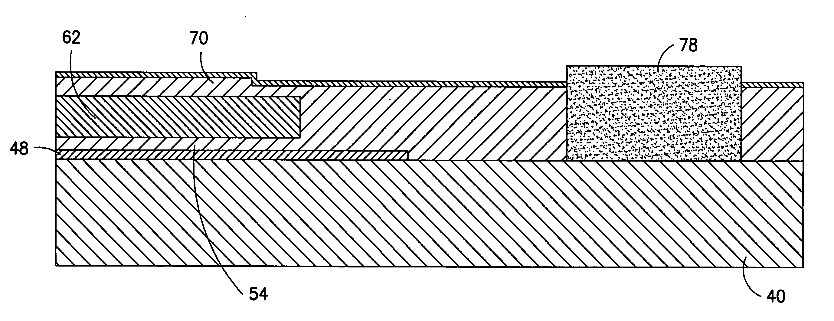
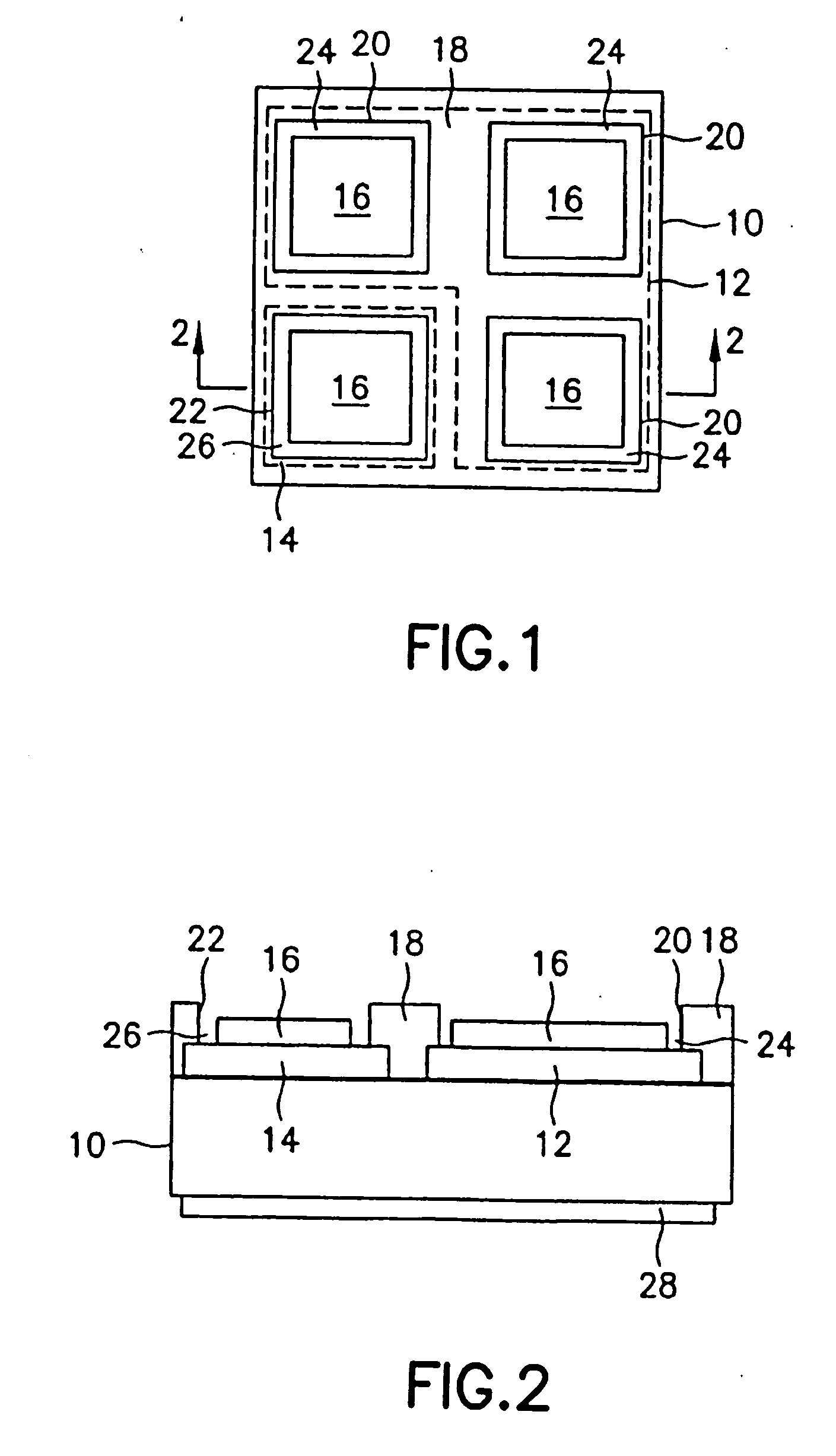
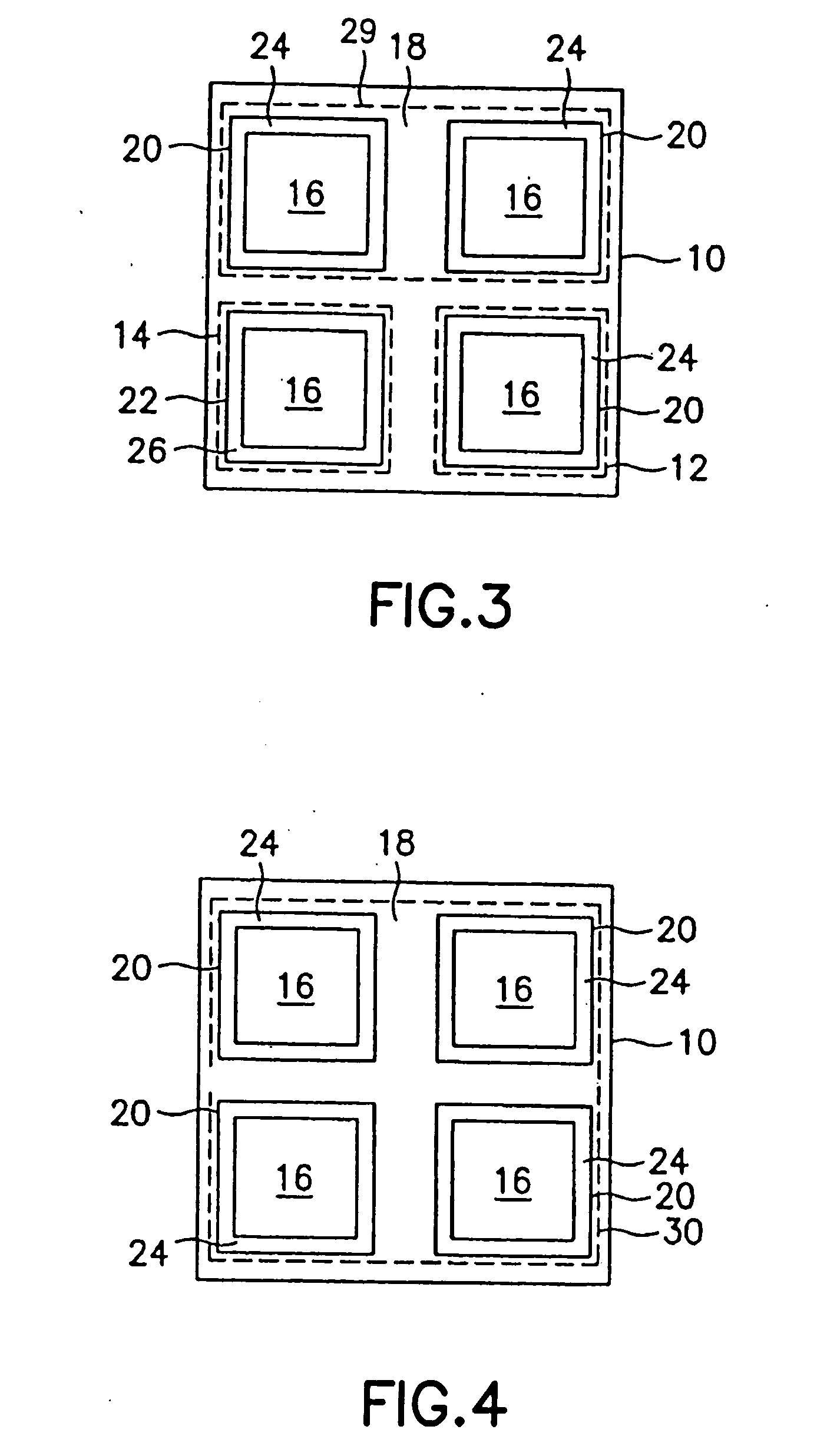
[0029] Referring to FIGS. 1 and 2, an example of a semiconductor package component fabricated according to the present invention includes a semiconductor die 10 having first power electrode 12 and control electrode 14 on a first major surface thereof. In the preferred embodiment, die 10 includes at least one solderable body 16 formed on first power electrode 12, at least one solderable body 16 formed on control electrode 14, and a passivation body 18 disposed on first power electrode 12 and control electrode 14. Passivation body 18 includes opening 20 to expose solderable body 16 on first power electrode 14 and opening 22 to expose solderable body 16 on control electrode 14. In the preferred embodiment, electrodes 12, 14 are formed from aluminum or aluminum silicon, and solderable bodies 16 are formed from a trimetal stack or any solderable material. The trimetal stack may include a silver layer at the top thereof, such as Ti / Pd / Ag trimetal stack.

[0030] Opening 20 may be wider than...


PUM


Abstract

A semiconductor package fabrication method in which drop on demand deposition of a drop on demand depositable material is used to prepare one component or a plurality of components of a semiconductor package or multi-chip module.

Description

RELATED APPLICATION [0001] This application is based on and claims benefit of U.S. Provisional Application Ser. No. 60 / 658,607, filed on Mar. 4, 2005, entitled DEPOSITING PASSIVATIONS USING JETTING TECHNOLOGY (INK-JETTING), to which a claim of priority is hereby made and the disclosure of which is incorporated by reference.BACKGROUND OF THE INVENTION [0002] The present invention relates to semiconductor package manufacturing and semiconductor packages. [0003] To fabricate a semiconductor package typically the components thereof must be treated. For example, in U.S. application Ser. No. 11 / 138,141, assigned to the assignee of the present invention, a method of fabricating a package is disclosed in which the front surface of the semiconductor die is subjected to a multi-step process whereby it receives a passivation body before the die is assembled in a conductive can. [0004] In a process according to the present invention, a drop on demand deposition technique is used to form a body ...

Claims


Application Information

Patent Timeline
IPC IPC(8): H01L21/00
CPCH01L21/4825H01L21/4867H01L23/544H01L24/06H01L24/13H01L24/14H01L24/27H01L24/29H01L24/33H01L24/743H01L24/83H01L25/16H01L25/50H01L2223/54433H01L2223/54486H01L2224/13099H01L2224/16H01L2224/274H01L2224/29H01L2224/2919H01L2224/29339H01L2224/743H01L2224/83192H01L2224/83194H01L2224/838H01L2924/01003H01L2924/01004H01L2924/01005H01L2924/01013H01L2924/01015H01L2924/01022H01L2924/01029H01L2924/01033H01L2924/01042H01L2924/01046H01L2924/01047H01L2924/0105H01L2924/01075H01L2924/01078H01L2924/01079H01L2924/01082H01L2924/0781H01L2924/1033H01L2924/13055H01L2924/13091H01L2924/14H01L2924/19041H01L2924/19042H01L2924/19043H05K1/0266H05K3/1241H05K3/245H01L2924/01006H01L2924/01023H01L2924/014H01L2924/0665H01L2224/29101H01L2924/0133H01L2924/157H01L2224/29111H01L2224/2929H01L2924/00013H01L2924/13064H01L2924/13062H01L2924/1305H01L2924/00H01L2924/00014H01L2224/29099H01L2224/05553H01L2224/05554H01L2224/0603H01L2224/0401H01L24/24H01L24/82H01L2224/24137H01L24/40
Inventor STANDING, MARTINPAVIER, MARKCLARKE, ROBERT J.SAWLE, ANDREWMCCARTNEY, KENNETH
Owner INFINEON TECH AMERICAS CORP
Why Eureka
Try Eureka