Side-emitting LED package having scattering area and backlight apparatus incorporating the LED lens

a technology of led package and led lens, which is applied in the direction of grinding head, lighting and heating apparatus, instruments, etc., can solve the problems of unsatisfactory reflection of light, increased manufacturing time and cost of backlight device, and undermining reliability of backlight device, so as to prevent light loss

Active Publication Date: 2006-09-21
SAMSUNG ELECTRONICS CO LTD
View PDF10 Cites 76 Cited by
  • Summary
  • Abstract
  • Description
  • Claims
  • Application Information

AI Technical Summary

Benefits of technology

[0025] It is further another object of the invention to provide a side-emitting LED package which can diffuse some portion of light emitted upward through a reflecting surface by applying scattering material on the reflecting surface, and a backlight apparatus incorporating the LED lens.
[0026] It is yet another

Problems solved by technology

Meanwhile, such reflecting paper attached may lead to undesired reflection of light L3.
To attach the reflecting paper is a delicate manual job that can be hardly automated, thus increasing the manufacture time and cost for the backlight device.
Moreover, the re

Method used


Image

  • Side-emitting LED package having scattering area and backlight apparatus incorporating the LED lens
  • Side-emitting LED package having scattering area and backlight apparatus incorporating the LED lens
  • Side-emitting LED package having scattering area and backlight apparatus incorporating the LED lens

Examples


second embodiment

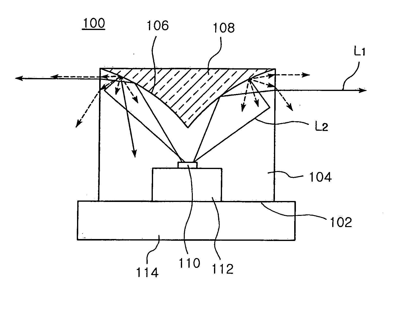
[0069]FIG. 8 illustrates the LED package of the invention. Referring to FIG. 8, the LED package 100A of the invention is substantially identical to the LED package 100 of FIG. 4 except that the former has a scattering film 108A applied on a reflecting surface 106. The scattering film 108A is made of materials substantially identical to the scattering area 108 of FIG. 4. Thus, the scattering film 108A can transmit / reflect light while scattering / diffusing it. In addition, transmissibility and reflectivity can be controlled by adjusting properties of the scattering particles.

[0070] Thereby, the scattering film 108A requires a less amount of the scattering particles and a binder forming the scattering film 108A than the scattering area 108 of the LED package 100 of FIG. 4. Also, the scattering film 108A of FIG. 8 has a uniform thickness, in general so that light can be transmitted at a uniform intensity across the film.

third embodiment

[0071]FIG. 9 shows the LED package of the invention. Referring to FIG. 9, the LED package 200 of the invention includes a bottom surface 202, first and second light exiting surfaces 204 and 206 cylindrically extended from the bottom surface 202 and a reflecting surface 208 positioned on an opposite side of the bottom surface 202. The reflecting surface 206 is symmetrical around a central axis A of the package 200 such that light incident from the bottom surface 202 is reflected toward the light exiting surface 204. Further, the first light exiting surface 204 is extended in a smooth convex curve from the bottom surface 202 and the second light exiting surface 206 is extended from the first light exiting surface 204 to an edge of the reflecting surface 208, obliquely slanted with respect to the central axis A of the package.

[0072] Also, the LED package 200 of the invention further comprises a scattering area 210 formed on the reflecting surface 208. The reflecting surface 202 has a f...

fourth embodiment

[0074]FIG. 10 shows the LED package of the invention. Referring to FIG. 10, the LED package 200A of the invention is substantially identical to the LED package 200 of FIG. 9 except that the former has a scattering film 210A applied on the reflecting surface 208.

[0075] As a result, a less amount of scattering particles and binder can be used to form the scattering film 210A than the scattering area 210 of the LED package 200 of FIG. 9. In addition, the scattering film 210A of FIG. 10 has a uniform thickness, in general so that light is transmitted at a uniform intensity across the film.

[0076] Then, with reference to FIG. 11, an explanation will be given regarding a process of forming a scattering area 108 in the side-emitting LED package 100 of FIG. 4.

[0077] First, with reference to FIG. 11(a), the LED package 100 as shown in FIG. 4 is prepared, which includes a bottom surface 102, a light exiting surface 104 cylindrically extended from the bottom surface 102 and a reflecting surfa...


PUM


Abstract

The invention provides an LED package and a backlight device incorporating the LED lens. The LED package has a bottom surface and a light exiting surface cylindrically extended around a central axis of the package from the bottom surface. Also, a reflecting surface is positioned on an opposite side of the bottom surface and symmetrical around the central axis such that light incident from the bottom surface is reflected toward the light exiting surface. Further, a scattering area is formed on the reflecting surface. According to the invention, by applying scattering materials on the reflecting surface of the LED package, a reflecting paper does not need to be attached, thereby simplifying a process and reducing the manufacture time and cost.

Description

CLAIM OF PRIORITY [0001] This application claims the benefit of Korean Patent Application No. 2005-22604 filed on Mar. 18, 2005, in the Korean Intellectual Property Office, the disclosure of which is incorporated herein by reference. BACKGROUND OF THE INVENTION [0002] 1. Field of the Invention [0003] The present invention relates to a light-emitting diode (LED) package for a backlight device. More particularly, the present invention relates to a side-emitting LED package having scattering material applied on a reflecting surface, and a backlight device incorporating the LED lens. [0004] 2. Description of the Related Art [0005] Applications using a light emitting diode (LED) as a light source are found in an LCD backlight device (system), a lighting device and the like. Also, in broader applications, an optical package may be employed in the LED to further enhance its efficiency and functions. [0006]FIG. 1 shows an example of an LED package for an LCD backlight device. [0007] The LED...

Claims


Application Information

Patent Timeline
IPC IPC(8): H01L33/00H01L33/56F21S2/00F21Y101/02H01L33/60
CPCG02F1/133603G02F1/133615H01L33/54H01L33/60H01L2933/0091B24B7/18B24B23/02B24B27/0007B24B27/0061B24B41/002B24D7/066
Inventor KIM, BUM JINKIM, HYUNG SUKAHN, HO SIKJEONG, YOUNG JUNEYANG, SUNG MIA
Owner SAMSUNG ELECTRONICS CO LTD
Why Eureka
Try Eureka