Arrangement method of metal electrode and transparent electrode in optical waveguide device and optical modulator using the optical waveguide

a technology of optical waveguide and metal electrode, which is applied in the direction of optical waveguide light guide, instruments, optics, etc., can solve the problems of direct modulation, difficulty in application, and difficulty in high-speed modulation at several ghz or mor

Inactive Publication Date: 2005-02-08
CORLUX CORP
View PDF12 Cites 15 Cited by
  • Summary
  • Abstract
  • Description
  • Claims
  • Application Information

AI Technical Summary

Benefits of technology

[0011]Accordingly, it is an object of the present invention to provide an optical modulator and an optical waveguide device that can modulate higher than conventional ways.
[0027]In accordance with the present invention as described above, it becomes possible to prevent optical loss and to achieve further high-speed modulation by forming a metal electrode in another part except a part formed on the optical waveguide in a transparent electrode. Of course, a part of the metal electrode may be arranged with being superimposed on the part formed on the optical waveguide in the transparent electrode. It will be desirable to limit a degree of superposition to a minimum necessary degree without performing full superimposition as in a conventional way.
[0028]The invention is particularly advantageous since it becomes possible to prevent optical loss and to achieve further high-speed modulation by forming a metal electrode so that the metal electrode may not be superimposed as much as possible on a part formed on an optical waveguide in a transparent electrode. Other features and advantages of the present invention will be apparent from the following description taken in conjunction with the accompanying drawings, in which like reference characters designate the same or similar parts throughout the figures thereof.

Problems solved by technology

However, in this direct modulation, a high-speed modulation at several GHz or more is difficult because of influences such as relaxation oscillation.
In addition, this direct modulation has a demerit such as difficulty of application to long-distance transmission since wavelength variation occurs.
However, when the electrode section has such three-layer structure, light leaks out from the transparent electrode to the metal electrode, and in particular, under high-speed modulation, optical loss caused by leaking out cannot be disregarded.
Hence, although it is desirable to constitute an electrode only with a transparent electrode, it becomes impossible to perform wire bonding etc. without a metal electrode, and hence an optical modulator cannot be substantially constituted.

Method used


Image

  • Arrangement method of metal electrode and transparent electrode in optical waveguide device and optical modulator using the optical waveguide
  • Arrangement method of metal electrode and transparent electrode in optical waveguide device and optical modulator using the optical waveguide
  • Arrangement method of metal electrode and transparent electrode in optical waveguide device and optical modulator using the optical waveguide

Examples


Embodiment Construction

class="d_n">[0046]FIG. 13B is a sectional view showing an embodiment where electrodes corresponding to respective optical waveguides are provided outside a plurality of optical waveguides;

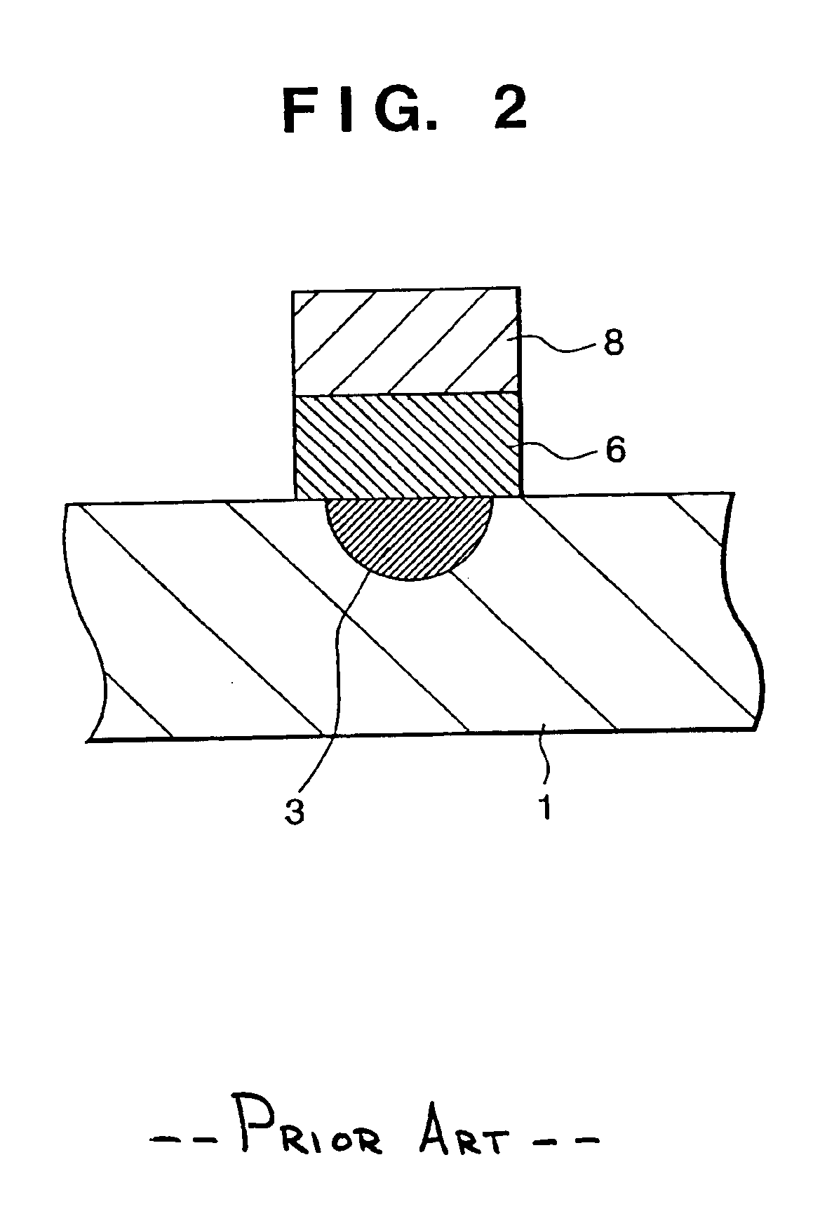
[0047]FIG. 14 is a sectional view showing an embodiment where an electrode that is not above an optical waveguide is formed by stacking a conductive transparent film and a metal film;

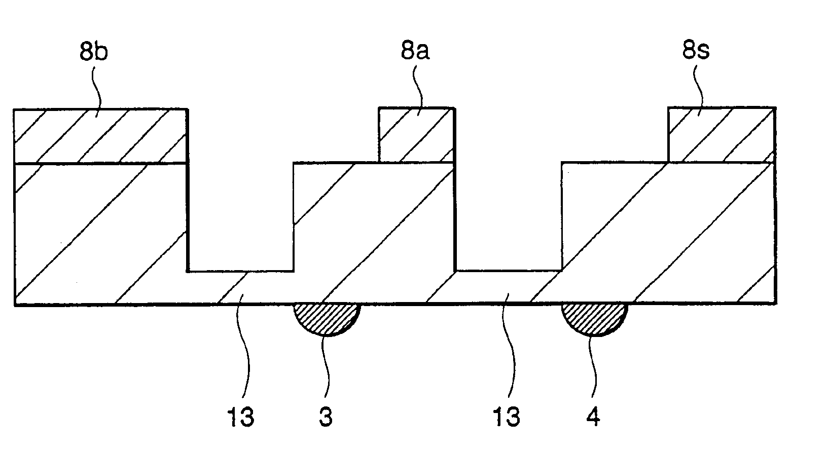
[0048]FIG. 15 is a sectional view showing an embodiment where grooves are formed between pluralities of electrodes;

[0049]FIG. 16 is a sectional view showing an embodiment where steps are provided between pluralities of electrodes;

[0050]FIG. 17 is a sectional view showing an embodiment where pluralities of conductive transparent films are connected with thinner conductive transparent films;

[0051]FIG. 18 is a sectional view showing an embodiment where a part of a metal film may cross an optical waveguide; and

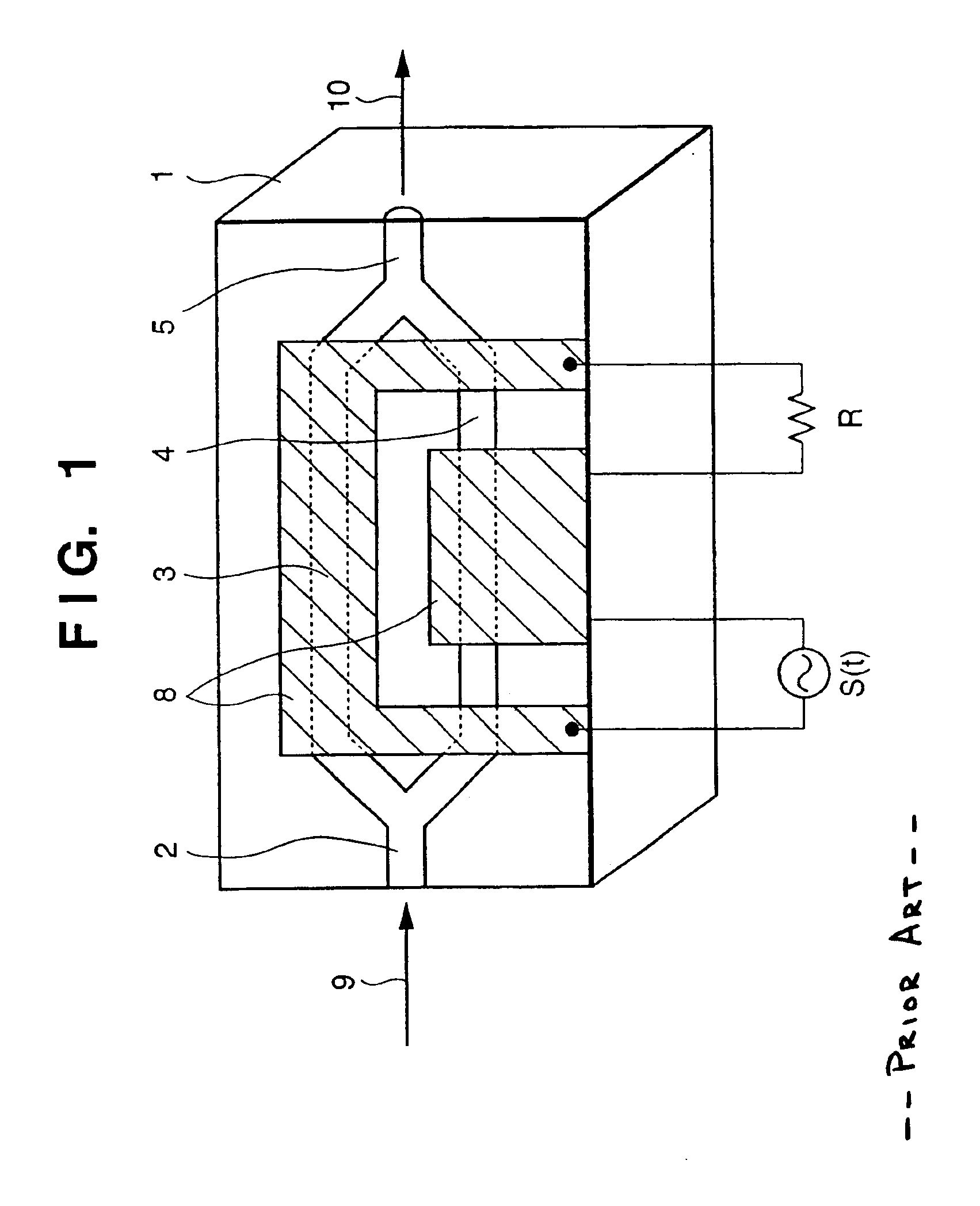
[0052]FIG. 19 is a top view showing a case where any one of the embodiments of the present invention is adopted in...


PUM

PropertyMeasurementUnit
impedanceaaaaaaaaaa
electro-optical effectaaaaaaaaaa
electric fieldaaaaaaaaaa

Abstract

The present disclosure relates to a device for modulating light emitted by a laser, including an optical substrate that has an electro-optical effect, at least one optical waveguide formed near a front face of the optical substrate, a first electrode that is formed with a conductive transparent film so that a part of the optical waveguide may be covered and is used for applying an electric field to the optical waveguide, a second electrode that is paired with the first electrode and is used for applying an electric field to the optical waveguide, and a third electrode that is formed with a metal film in a position that is shifted from a position just above the optical waveguide and is electrically connected with the first electrode.

Description

FIELD OF THE INVENTION[0002]This invention relates to an optical waveguide device used in fields such as optical communication, optical information processing, and optical signal processing, and more particularly, to an optical waveguide type optical modulator that performs modulation by using the optical waveguide provided in a substrate.BACKGROUND OF THE INVENTION[0003]The needs of acceleration of optical transmission systems have been increasingly growing with the explosive diffusion of the Internet. An optical signal of a general system is obtained by directly modulating the injection current of a semiconductor laser or a light emitting diode. This is called direct modulation. However, in this direct modulation, a high-speed modulation at several GHz or more is difficult because of influences such as relaxation oscillation. In addition, this direct modulation has a demerit such as difficulty of application to long-distance transmission since wavelength variation occurs.[0004]As ...

Claims


Application Information

Patent Timeline
Patent Type & Authority Patents(United States)
IPC IPC(8): G02F1/035G02F1/01G02F1/225G02B6/12
CPCG02F1/035G02F1/225G02F2201/12
Inventor SEINO, MINORU
Owner CORLUX CORP
Why Eureka
Try Eureka