Semiconductor device and method of fabricating the same

Inactive Publication Date: 2014-11-20
SEOUL VIOSYS CO LTD
View PDF10 Cites 15 Cited by
  • Summary
  • Abstract
  • Description
  • Claims
  • Application Information

AI Technical Summary

Benefits of technology

[0060]Meanwhile, an LED including an active layer as a semi-polar semiconductor layer is provided, so that polarization can be reduced or removed, thereby improving light emitting efficiency. Further, semiconductor layers are grown using a miscut GaN substra

Problems solved by technology

However, the epitaxial layer grown on the heterogeneous substrate has a relatively higher dislocation density due to lattice mismatch between the epitaxial layer and the growth substrate and a difference in thermal expansion coefficient between the epitaxial layer and the growth substrate.
There is a limitation in improving the light emitting efficiency of the LED using the epitaxial layer having such a high dislocation density.
Therefore, the recombination rate of electrons

Method used


Image

  • Semiconductor device and method of fabricating the same
  • Semiconductor device and method of fabricating the same
  • Semiconductor device and method of fabricating the same

Examples


Example

[0079]Hereinafter, preferred embodiments of the present invention will be described in detail with reference to the accompanying drawings. The following embodiments are provided only for illustrative purposes so that those skilled in the art can fully understand the spirit of the present invention. Therefore, the present invention is not limited to the following embodiments but may be implemented in other forms. In the drawings, the widths, lengths, thicknesses and the like of elements are exaggerated for convenience of illustration. Like reference numerals indicate like elements throughout the specification and drawings.

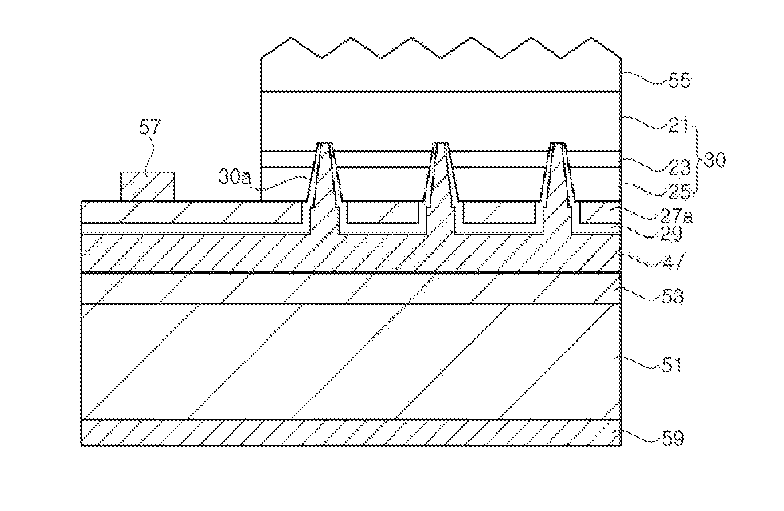
[0080]FIG. 1 is a sectional view illustrating a light emitting diode (LED) according to an embodiment of the present invention.

[0081]Referring to FIG. 1, the LED may include a support substrate 31, a semiconductor stack 30, a p-electrode layer 27, a bonding metal 33, a transparent oxide layer 35 and an n-electrode pad 37. The LED may further include a bonding pad 39...


PUM


Abstract

Disclosed are a semiconductor device and a method of fabricating the same. The method includes forming a first GaN layer, a sacrificial layer and a second GaN layer on a GaN substrate, wherein the sacrificial layer has a bandgap narrower than those of the GaN layers; forming a groove penetrating the second GaN layer and the sacrificial layer; growing GaN-based semiconductor layers on the second GaN layer to form a semiconductor stack; forming a support substrate on the semiconductor stack; and removing the GaN substrate from the semiconductor stack by etching the sacrificial layer. Accordingly, since the sacrificial layer is etched using the groove, the support substrate can be separated from the semiconductor stack without damaging the support substrate.

Description

CROSS-REFERENCE TO RELATED APPLICATIONS[0001]This application is the National Stage of International Application No. PCT / KR2012 / 010852, filed on Dec. 13, 2012, and claims priority from and the benefit of Korean Patent Application No. 10-2011-0134130, filed on Dec. 14, 2011, Korean Patent Application No. 10-2011-0135513, filed on Dec. 15, 2011, Korean Patent Application No. 10-2012-0026879, filed on Mar. 16, 2012, and Korean Patent Application No. 10-2012-0026948, filed on Mar. 16, 2012, which are hereby incorporated by reference for all purposes as if fully set forth herein.BACKGROUND[0002]1. Field[0003]The present invention relates to a semiconductor device and a method of fabricating the same, and more particularly, to a light emitting diode and a method of fabricating the same.[0004]2. Discussion of the Background[0005]In general, since Group III nitrides such as gallium nitride (GaN) and aluminum nitride (AlN) have excellent thermal stability and a direct-transition-type energy ...

Claims


Application Information

Patent Timeline
IPC IPC(8): H01L33/32H01L33/00H01L33/42H01L33/38H01L33/22
CPCH01L33/32H01L33/38H01L33/0075H01L33/42H01L33/22H01L33/007H01L33/025H01L33/382
Inventor SEO, WON CHEOLCHO, DAE SUNGLEE, CHUNG HOONNAM, KI BUM
Owner SEOUL VIOSYS CO LTD
Why Eureka
Try Eureka