Thermal interface structure and process for making the same

a technology of thermal interface and thermal interface structure, which is applied in the direction of semiconductor devices, electrical devices, semiconductor/solid-state device details, etc., can solve the problems of reducing the flexibility of the base material, affecting the heat dissipation efficiency between the electronic component and the cooling device, and the type of thermal interface structure can only be manufactured at high cos

Inactive Publication Date: 2006-09-21
TSINGHUA UNIV +1
View PDF16 Cites 68 Cited by
  • Summary
  • Abstract
  • Description
  • Claims
  • Application Information

AI Technical Summary

Benefits of technology

[0006] Another kind of thermal interface structure has recently been developed. The thermal interface structure is obtained by fixing carbon nanotubes in a polymer by injection molding. The carbon nanotubes are distributed directionally, and each carbon nonotube provides a heat conduction path. A heat conduction coefficient of this kind of thermal interface structure can be 6600 W / niK at room temperature, as disclosed in an article entitled “Unusually High Thermal Conductivity of Carbon Nanotubes” by Savas Berber (page 4613, Vol. 84, Physical Review Letters 2000). However, this kind of the thermal interface structure can only be manufactured at high cost, because only one thermal interface structure can be formed by an injection molding process. Furthermore, the unwanted polymer must be removed by an etching method or a mulling method so that ends of the carbon nanotubes can be exposed to enhance the heat conduction coefficient.

Problems solved by technology

Thus, the heat dissipation efficiency between the electronic component and the cooling device is greatly impacted by poor contact between dissipation surfaces.
However, the flexibility of the base material decreases as the quantity of particles is increased, this effects the contact between the surfaces and thus effects the heat conduction.
However, this kind of the thermal interface structure can only be manufactured at high cost, because only one thermal interface structure can be formed by an injection molding process.
Therefore, a heretofore unaddressed need exists in the industry for a method which can address the aforementioned deficiencies and inadequacies with respect to thermal interface structure and method of manufacturing of the same.

Method used


Image

  • Thermal interface structure and process for making the same
  • Thermal interface structure and process for making the same
  • Thermal interface structure and process for making the same

Examples


Embodiment Construction

[0020] Reference will now be made to the drawings to describe embodiments of the present thermal interface structure and its method of manufacture in detail.

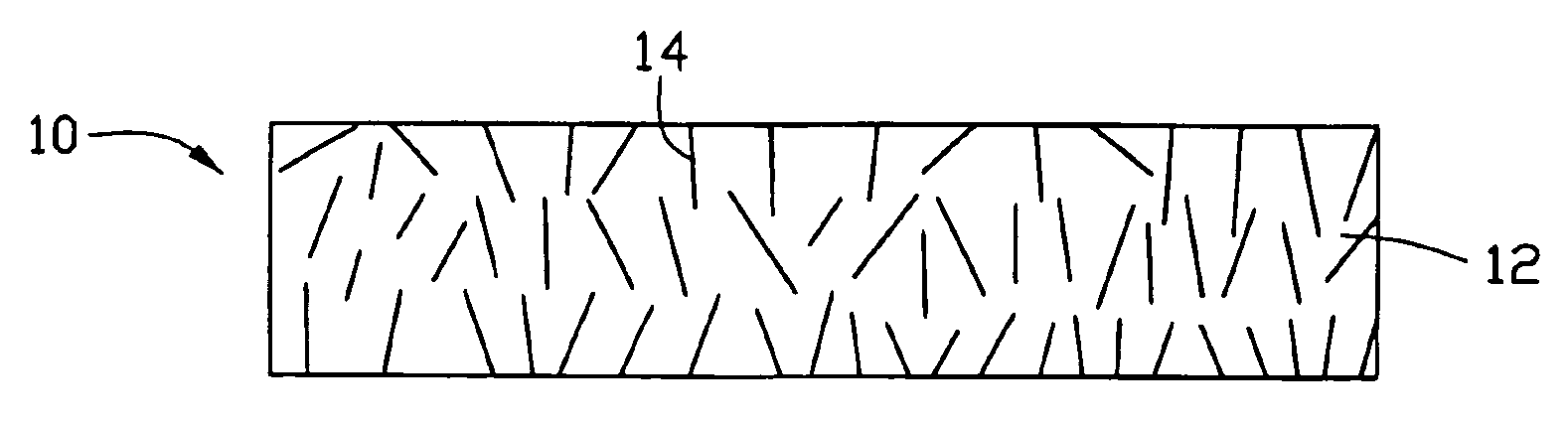
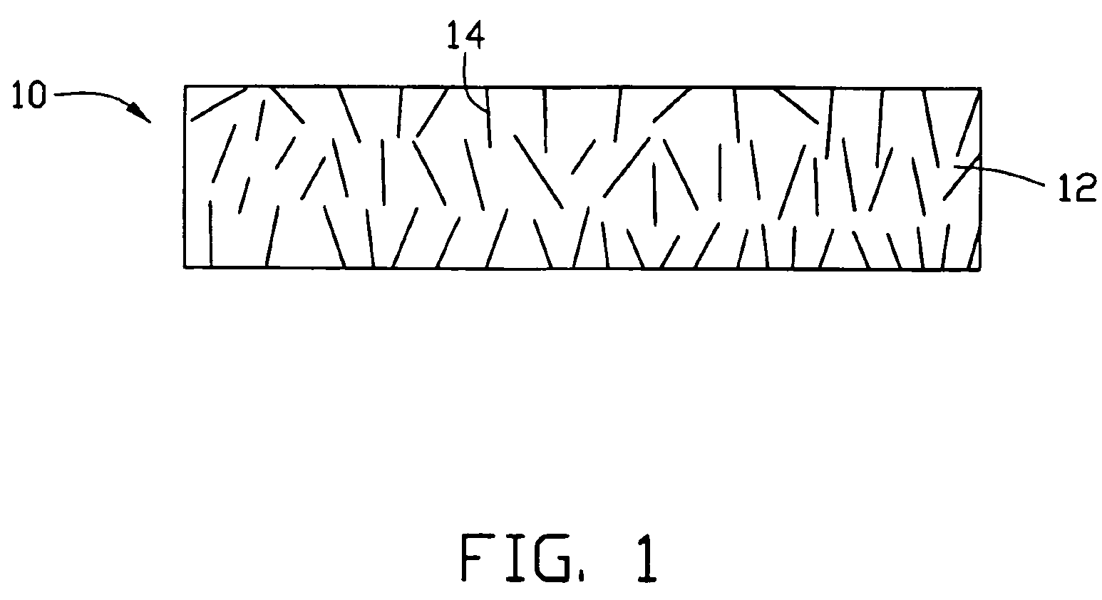
[0021] Referring to FIG. 1, a thermal interface structure 10 in accordance with a preferred embodiment of the present thermal interface structure is shown. The thermal interface structure 10 is generally adapted for being disposed between electronic components (not shown) such as central processing units (CPUs), and cooling devices (not shown) such as heat sinks, to dissipate heat generated by the electronic components. The thermal interface structure 10 comprises a matrix 12 and a plurality of carbon nanotubes 14 incorporated in the matrix 12.

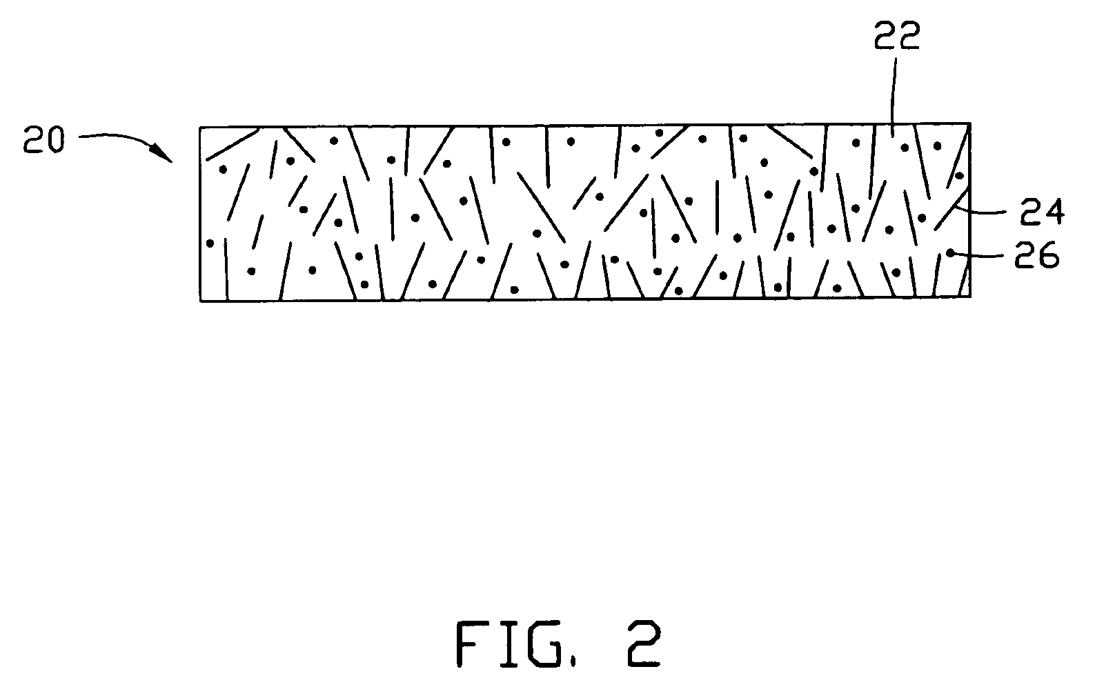
[0022] The matrix 12 is made from a phase change material with a solid to liquid phase-change temperature in the range of 50° C.˜60° C. (e.g. paraffin material). The nanotubes 14 are dispersed in the matrix 12 randomly. Preferably, the percent by mass of the nanotubes 14 is in the range ...


PUM

PropertyMeasurementUnit
temperatureaaaaaaaaaa
thicknessaaaaaaaaaa
percent by massaaaaaaaaaa

Abstract

A thermal interface structure (10, 20) is provided for a highly conductive thermal interface between an electronic component and a cooling device for dissipating heat generated by the electronic component. The thermal interface structure includes a matrix (12, 22) and a plurality of carbon nanotubes (14, 24) incorporated in the matrix. The matrix is generally made from a phase change material. A method for making a thermal interface structure is also provided.

Description

BACKGROUND [0001] 1. Technical Field [0002] The invention relates generally to thermal interface structures, and more particularly to a thermal interface structure that employs carbon nanotubes to reduce thermal resistance between an electronic component, such as a central processing unit (CPU), and a cooling device, such as a heat sink. The invention also relates to a process for forming a thermal interface structure. [0003] 2. Discussion of Related Art [0004] With the continually decreasing size of electronic and micromechanical devices, increasing emphasis is laid on improving cooling, thus preventing from structural damage. Cooling devices, such as fans, heat sinks, water-cooling devices and heat pipes, are widely used. The cooling devices are directly assembled onto an electronic component, and a dissipation surface of each of the cooling devices touches a dissipation surface of the electronic component. Heat generated by the electronic component is transmitted to the cooling d...

Claims


Application Information

Patent Timeline
Patent Type & Authority Applications(United States)
IPC IPC(8): H01L23/34H01L21/00
CPCH01L23/373H01L23/4275H01L2924/0002H01L2924/00
Inventor LIU, CHANG-HONGFAN, SHOU-SHAN
Owner TSINGHUA UNIV
Why Eureka
Try Eureka