Semiconductor cleaning apparatus and semiconductor cleaning method

a cleaning apparatus and semiconductor technology, applied in the direction of cleaning process and apparatus, cleaning using liquids, semiconductor/solid-state device testing/measurement, etc., can solve the problems of disadvantageous starting of the next wafer processing step without satisfying the desired cleanliness factor, and disadvantageous ending of the rinse process

Inactive Publication Date: 2006-09-28
KK TOSHIBA
View PDF4 Cites 19 Cited by
  • Summary
  • Abstract
  • Description
  • Claims
  • Application Information

AI Technical Summary

Benefits of technology

[0008] A semiconductor cleaning apparatus according to the present invention comprises: a particle monitor which measures the number of particles in a processing liquid used in a rinse process after a semiconductor wafer is subjected to a cleaning process by means of the processing liquid; a specific resistance measuring unit which measures a specific resistance of the processing liquid used in the rinse process; and a control unit which determines an end point at which the rinse process is completed on the basis of the number of particles measured by the particle monitor and the specific resistance measured by the specific resistance measuring unit to en

Problems solved by technology

For this reason, the next step in the wafer processing is disadvantageously started without satisfying a desired cleanliness factor.
Furthermore, in the conventional technique, since the rinse process is ended regardless of a stickin

Method used


Image

  • Semiconductor cleaning apparatus and semiconductor cleaning method
  • Semiconductor cleaning apparatus and semiconductor cleaning method
  • Semiconductor cleaning apparatus and semiconductor cleaning method

Examples


first embodiment

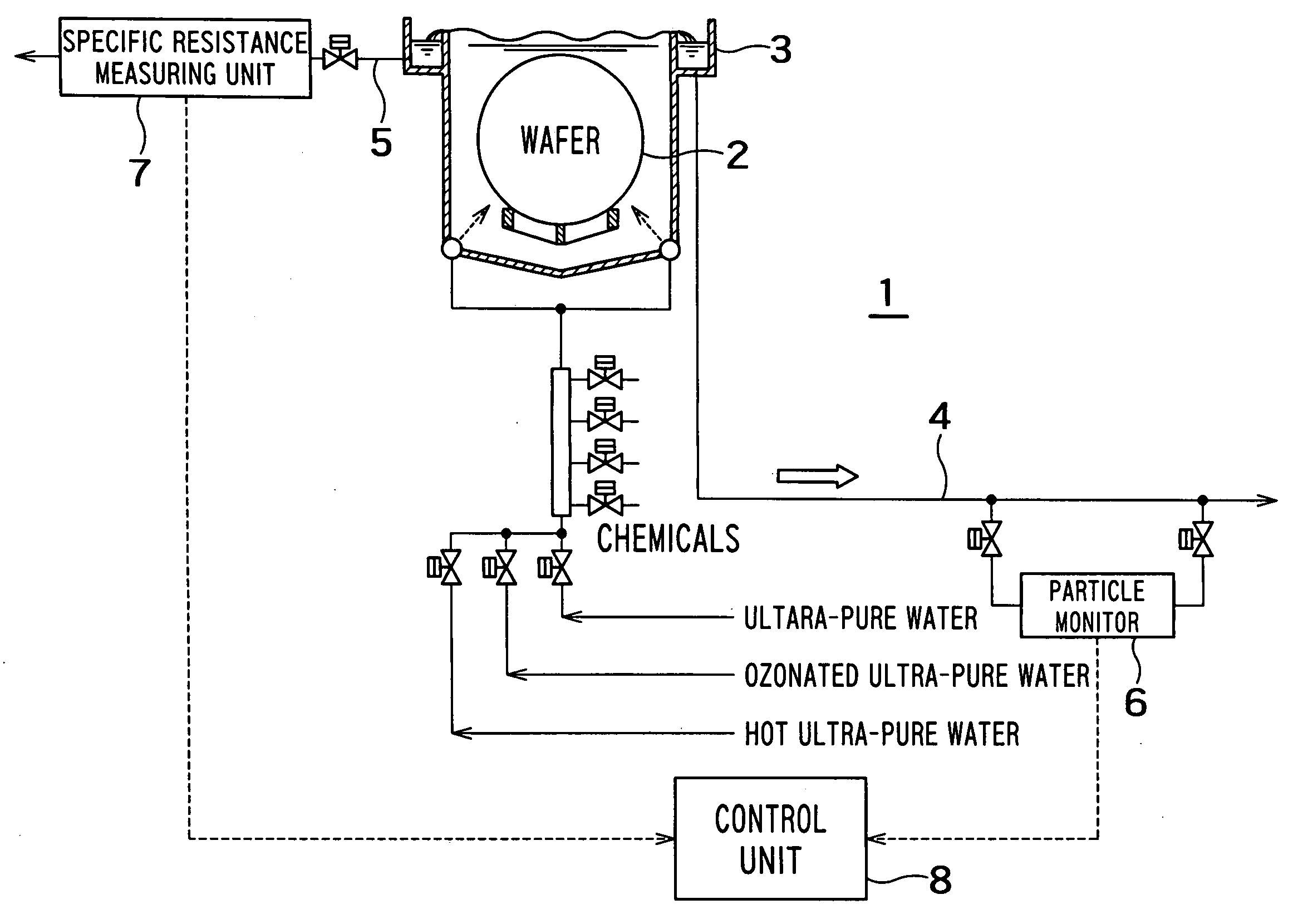
[0020]FIG. 1 shows a configuration of embodiment a main part of a semiconductor cleaning apparatus according to a first embodiment of the present invention.

[0021] A semiconductor cleaning apparatus 1 includes: a processing tank 3 to perform a cleaning process and a rinse process; a particle monitor 6 serving as a particle counting unit arranged in a bypass pipe of a first drain pipe 4 to measure the number of particles in processing liquid used in a rinse process; a specific resistance measuring unit 7 serving as a specific resistance measuring means arranged in a second drain pipe 5 to measure a specific resistance of the processing liquid used in the rinse process; and a control unit 8 serving as a control unit which determines an end point at which the rinse process is completed on the basis of a measurement result of the particle monitor 6 and a specific resistance measured by the specific resistance measuring unit 7. The cleaning process mentioned here includes a process of re...

second embodiment

[0041] As described above, according to the configuration of the control unit 8 determines an end point of a rinse process on the basis of the number of particles and the specific resistance of a processing liquid used in the rinse process, the number of particles being measured by the particle monitor 6. The second embodiment will describe a configuration in which the control unit 8 determines an end point of a rinse process on the basis of the specific resistance and a difference between the first number of particles in a processing liquid used in the rinse process and the second number of particles in the processing liquid having a large cleanliness factor obtained before a cleaning process (i.e., a relative change of the number of particles).

[0042]FIG. 8 shows a configuration of a main part of a semiconductor cleaning apparatus according to a second embodiment of the present invention. In this embodiment, a particle monitor 6 is designed to further measure the number of particl...


PUM


Abstract

A semiconductor cleaning apparatus according to the present invention comprises: a particle monitor which measures the number of particles in a processing liquid used in a rinse process after a semiconductor wafer is subjected to a cleaning process by means of the processing liquid; a specific resistance measuring unit which measures a specific resistance of a processing liquid used in the rinse process; and a control unit which determines an end point at which the rinse process is completed on the basis of the number of particles measured by the particle monitor and the specific resistance measured by the specific resistance measuring unit to end the rinse process.

Description

CROSS-REFERENCE TO RELATED APPLICATION [0001] This application is based upon and claims the benefit of priority from prior Japanese Patent Application No. 2005-070711, filed on Mar. 14, 2005, the entire contents of which are incorporated herein by reference. BACKGROUND OF THE INVENTION [0002] 1. Field of the Invention [0003] The present invention relates to a semiconductor cleaning apparatus and a semiconductor cleaning method which controls a rinse process performed after completion of a cleaning process of a semiconductor wafer. [0004] 2. Background Art [0005] As a conventional semiconductor cleaning method, there is known a method in which a cleaning process for a semiconductor wafer is performed by trapping a cleaning chemical such as an SPM (Sulfuric Acid-hydrogen peroxide Mixture) or SC1 (ammonia-hydrogen peroxide mixture) in a cleaning tank, by sequentially overflowed the cleaning chemical in the cleaning tank by circularly supplying and by filtering the cleaning chemical at ...

Claims


Application Information

Patent Timeline
IPC IPC(8): B08B7/04B08B3/00
CPCB08B3/04B08B13/00H01L21/02052H01L21/67057H01L21/67253H01L22/12H01L22/26
Inventor UMEZAWA, KAORITOMITA, HIROSHI
Owner KK TOSHIBA
Why Eureka
Try Eureka