Semiconductor device and manufacturing method thereof
a technology of semiconductor devices and semiconductors, applied in the direction of semiconductor devices, semiconductor/solid-state device details, electrical apparatus, etc., can solve problems such as dish-shaped warpage, and achieve the effect of suppressing warpage of semiconductor devices
- Summary
- Abstract
- Description
- Claims
- Application Information
AI Technical Summary
Benefits of technology
Problems solved by technology
Method used
Image

Examples
first preferred embodiment
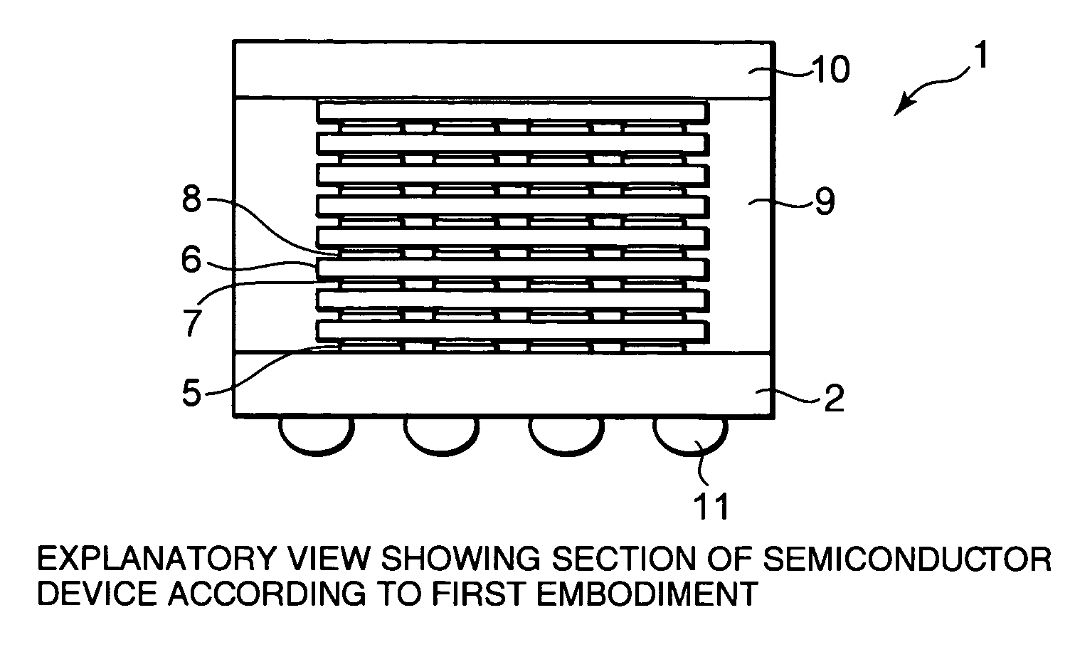
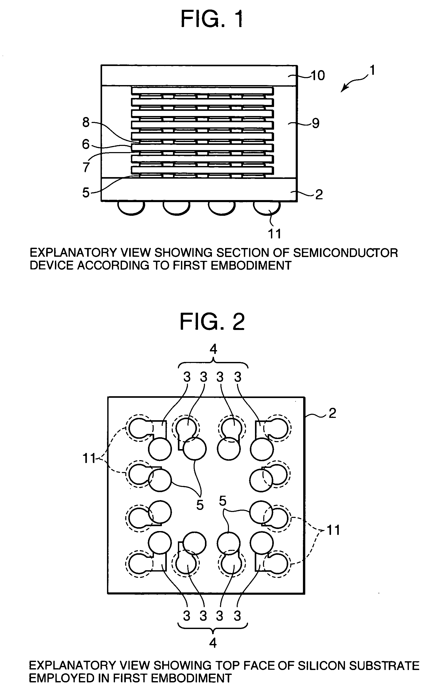
[0020]FIG. 1 is an explanatory view showing a cross section of a semiconductor device according to a first embodiment, and FIG. 2 is an explanatory view illustrating a top face of a silicon substrate employed in the first embodiment, respectively.
[0021] In FIG. 1, reference numeral 1 indicates the semiconductor device.
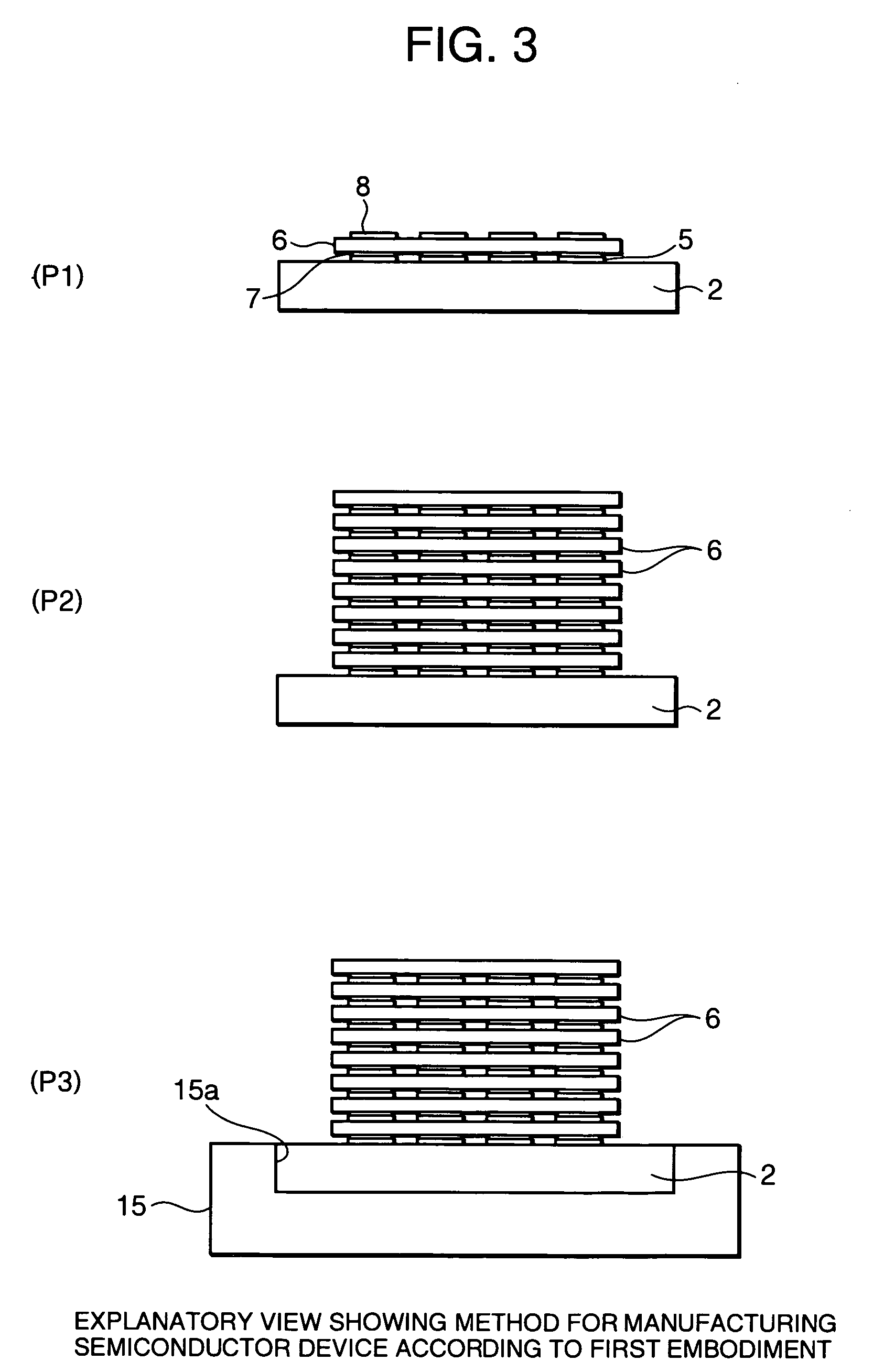
[0022] Reference numeral 2 indicates the silicon substrate used as a lower substrate. Wiring patterns that consist of a plurality of wirings 3 are formed in the top face of the silicon substrate. A plurality of substrate ball pads 5 are formed at predetermined portions or sections of the wirings 3.
[0023] Reference numerals 6 indicate semiconductor chips. A plurality of bumps 7 are respectively disposed on the lower surfaces of the semiconductor chips. A plurality of chip ball pads 8 are respectively disposed on the upper surfaces of the semiconductor chips. The bumps 7 of each semiconductor chip 6 corresponding to an undermost layer are electrically connected to the...
second preferred embodiment
[0055]FIG. 5 is an explanatory view showing a cross section of a semiconductor device according to a second embodiment, and FIG. 6 is an explanatory view showing a top face of a metal plate body employed in the second embodiment, respectively.
[0056] Incidentally, portions similar to the first embodiment are given the same reference numerals and their explanations are omitted.
[0057] In FIGS. 5 and 6, reference numeral 21 indicates a metal plate body used as an upper plate. The metal plate body is constituted by connecting a plurality of metal plates 10 similar to the first embodiment by means of slender or thin connecting portions 22 formed of the same material as the metal plates 10. The metal plate body is formed by punching out a plate member of substantially the same size as a silicon substrate 2 of the present embodiment, which is formed of the material of each metal plate 10, by a press machine.
[0058] The metal plate body 21 of the present embodiment is constituted in such a...
PUM
 Abstract
Description
Claims
Application Information
 - R&D Engineer
- R&D Manager
- IP Professional
- Industry Leading Data Capabilities
- Powerful AI technology
- Patent DNA Extraction
Browse by: Latest US Patents, China's latest patents, Technical Efficacy Thesaurus, Application Domain, Technology Topic.
© 2024 PatSnap. All rights reserved.Legal|Privacy policy|Modern Slavery Act Transparency Statement|Sitemap