Light-emitting diode package structure, cold cathode flourescent lamp and photoluminescent material thereof

a technology of light-emitting diodes and package structures, applied in the direction of discharge tubes/lamp details, luminescent compositions, discharge tubes/lamp details, etc., can solve the problems of high luminous efficiency, high production cost, and difficulty in some degree in producing and controlling light interfusing effects, so as to improve light interfusing effects, reduce production costs, and simplify the overall process of fabricating led packages

Active Publication Date: 2006-09-28
LEXTAR ELECTRONICS CORP
View PDF10 Cites 11 Cited by
  • Summary
  • Abstract
  • Description
  • Claims
  • Application Information

AI Technical Summary

Benefits of technology

[0011] According, the present invention is directed to provide an LED package structure to further enhance the light infusing effect thereof.
[0012] According, the present invention is to provide a cold cathode fluorescent lamp, wherein a photoluminescent material (PL material) is used to replace the conventional fluorescent layer and diffusion layer to enhance the light infusing effect thereof.
[0013] According, the present invention is to provide a PL material which is different from conventional fluorescent powder but suitable for the LED package structure and cold cathode fluorescent lamps to produce better light infusing effect.
[0023] The present invention uses a PL material to replace the conventional fluorescent layer and diffusion layer for light conversion and a light interfusing effect. Thus, there are no more match problems among the variants in the prior art, such as the materials of the fluorescent layer and diffusion layer, the particle size and the particle distribution density, and the like. Besides, the overall procedure for fabricating LED packages is effectively simplified along with a lower production cost and better light interfusing effect.

Problems solved by technology

This mode features a high luminous efficiency along with a higher production cost.
Since too many factors can influence the light interfusing effect, practically it is difficult to some extent to produce and control the light interfusing effect.

Method used


Image

  • Light-emitting diode package structure, cold cathode flourescent lamp and photoluminescent material thereof
  • Light-emitting diode package structure, cold cathode flourescent lamp and photoluminescent material thereof
  • Light-emitting diode package structure, cold cathode flourescent lamp and photoluminescent material thereof

Examples


first embodiment

The First Embodiment

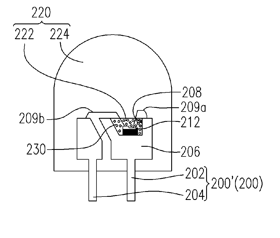
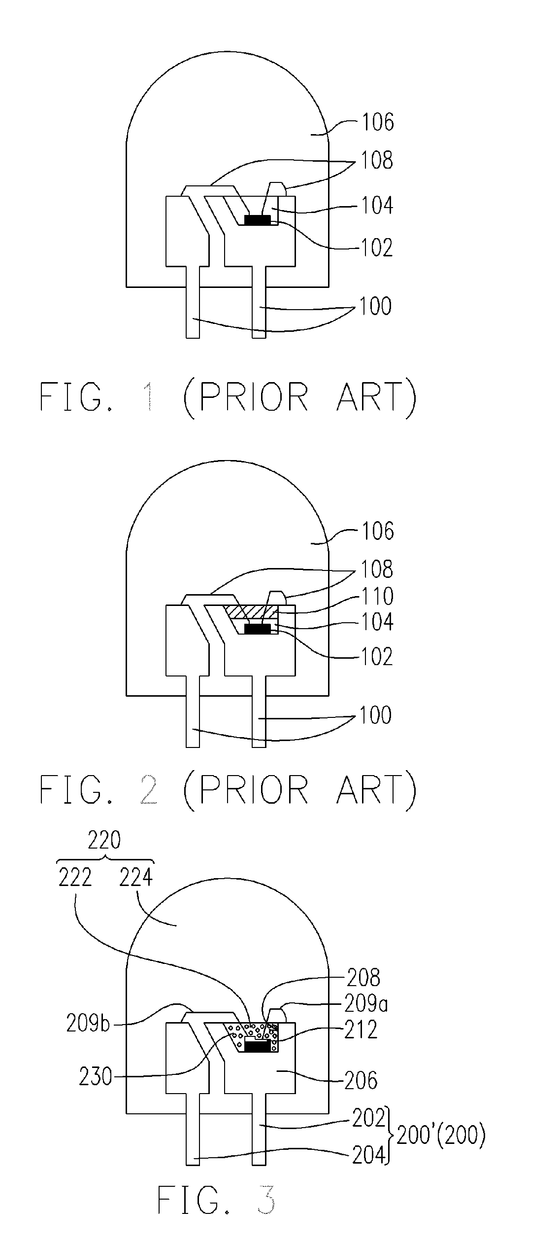
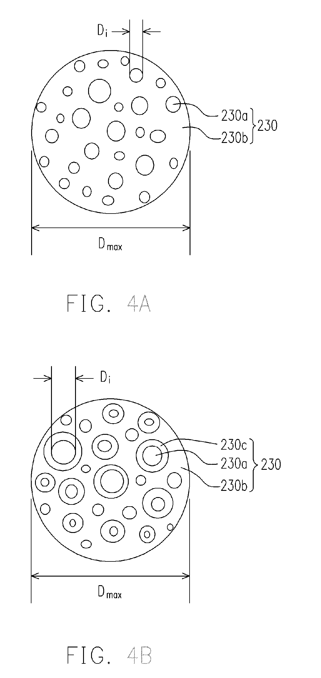
[0032]FIG. 3 is a schematic drawing of an LED package structure according to the first embodiment of the present invention. In FIG. 3, the LED package structure in the first embodiment of the present invention mainly comprises a carrier 200, an LED chip 210, an encapsulant 220 and a PL material 230, wherein the LED chip 210 is disposed on the carrier 200 to emit light; the encapsulant 220 encapsulates most of the carrier 200 and the LED chip 210 thereon; and the PL material 230 is evenly distributed in the encapsulant 220. The PL material layer 230 is suitable to be excited by the light emitted from the LED chip 210 and to scatter the light.

[0033] In the first embodiment, the carrier 200 is, for example, package lead pins 200′ as shown in FIG. 3. The package lead pins 200′ comprise a first lead pin 202 and a second lead pin 204. On the top of the first lead pin 202 is a carrier pad 206, comprising a chip-holding cell 208. The chip-holding cell 208 is of a concav...

second embodiment

The Second Embodiment

[0041]FIG. 6 and FIG. 7 are schematic drawings of white LED package structures according to the second embodiment of the present invention. In FIG. 6, the structure in the second embodiment is similar to that of the first embodiment. The difference in the second embodiment is that the carrier 300 therein is a printed circuit board (PCB) 300′ on which the package is disposed.

[0042] The LED package structure in the second embodiment mainly comprises a PCB 300′, an LED chip 310, an encapsulant 320 and a PL material 330. The encapsulant 320 similarly comprises an inner encapsulant 322 and an outer encapsulant 324, wherein the inner encapsulant 322 encapsulates the LED chip 310, and the outer encapsulant 324 encapsulates a portion of the PCB 300′, the LED chip 310, the inner encapsulant 322, the PL material 330 and the soldering wires 314. When the encapsulant 320 comprises only an outer encapsulant 324 without the inner encapsulant 322, the outer encapsulant 324 ca...

third embodiment

The Third Embodiment

[0046] In the first and second embodiment of the present invention, the PL material is used in the LED package structure. In addition, the PL material can also be used in general cold cathode fluorescent lamps to achieve a better light interfusing effect.

[0047]FIG. 8 is a schematic drawing of a cold cathode fluorescent lamp according to the third embodiment of the present invention. In FIG. 8, the cold cathode fluorescent lamp 400 comprises a light tube 410, a discharging gas (not shown in the figure), a PL material 420 and an electrode set 430, wherein the light tube 110 is properly filled with discharging gas, such as mercury vapor and inert gas. The PL material 420 is applied on the inner wall of the light tube 410. In addition, the electrode set 430 comprises both an anode and a cathode individually disposed at two ends of the light tube 410, respectively. The electrode set 430 is electrically connected to a power supply (not shown in the figure).

[0048] Whe...


PUM


Abstract

An LED package structure including a carrier, an LED chip, an encapsulant and a PL material is provided, wherein the LED chip is disposed on the carrier for emitting light. The encapsulant encapsulates the LED chip. The PL material is distributed in the encapsulant. The PL material is suitable for being excited by the light emitted from the LED chip and scattering the light. Moreover, the present invention provides a novel PL material with a molecular formula of WmMon(Y,Ce,Tb,Gd,Sc)3+t+u(Al,Ga,Tl,In,B)5+u+2v(O,S,Se)12+2t+3u+3v+3m+3n: Ce3+, Tb3+, wherein 0<t<5 and 0<m, n, u, v<15.

Description

CROSS-REFERENCE TO RELATED APPLICATION [0001] This application claims the priority benefit of Taiwan application serial no. 94109063, filed on Mar. 24, 2005. All disclosure of the Taiwan application is incorporated herein by reference. BACKGROUND OF THE INVENTION [0002] 1. Field of Invention [0003] The present invention relates to an LED (light-emitting diode) package structure. More particularly, it relates to an LED package structure comprising a photoluminescent diffuser material. [0004] 2. Description of the Related Art [0005] As LED luminous efficiency has continued to enhance in recent years, LEDs have gradually replaced fluorescent lamps and incandescent lamps in some applications, such as fast-responding scanner light sources, LCD (Liquid Crystal Display) back light sources, automobile dashboard lighting, traffic lights, and general lighting devices. In comparison with conventional light bulbs, LEDs have absolute predominance because of features, such as compact size, durabi...

Claims


Application Information

Patent Timeline
Patent Type & Authority Applications(United States)
IPC IPC(8): H01J1/62H01L33/50H01L33/56
CPCC09K11/7774H01L33/502H01L33/56H01L2933/0091H01L2924/181H01L2224/48247H01L2224/48257H01L2224/49107H01L2224/8592H01L2924/00012
Inventor CHANG, CHIH-CHINHSIEH, HSIANG-CHENGHUANG, TENG-HUEI
Owner LEXTAR ELECTRONICS CORP
Why Eureka
Try Eureka