
Memory device having shared open bit line sense amplifier architecture

a memory device and open-bit line technology, applied in the field of memory devices with shared open-bit line sense amplifier architecture, can solve the problems of reducing flexibility in the design of the layout of the sense amplifier sa, affecting one side of the bit line bl, and affecting one side of the pair of bit lines bl,

Inactive Publication Date: 2006-09-28
SAMSUNG ELECTRONICS CO LTD
View PDF3 Cites 25 Cited by
  • Summary
  • Abstract
  • Description
  • Claims
  • Application Information

AI Technical Summary

Benefits of technology

The patent describes a memory device with multiple memory cell arrays and a sense amplifier that can connect to bit lines in different arrays. The device can select specific bit lines to sense and operate on, improving efficiency and speed.

Problems solved by technology

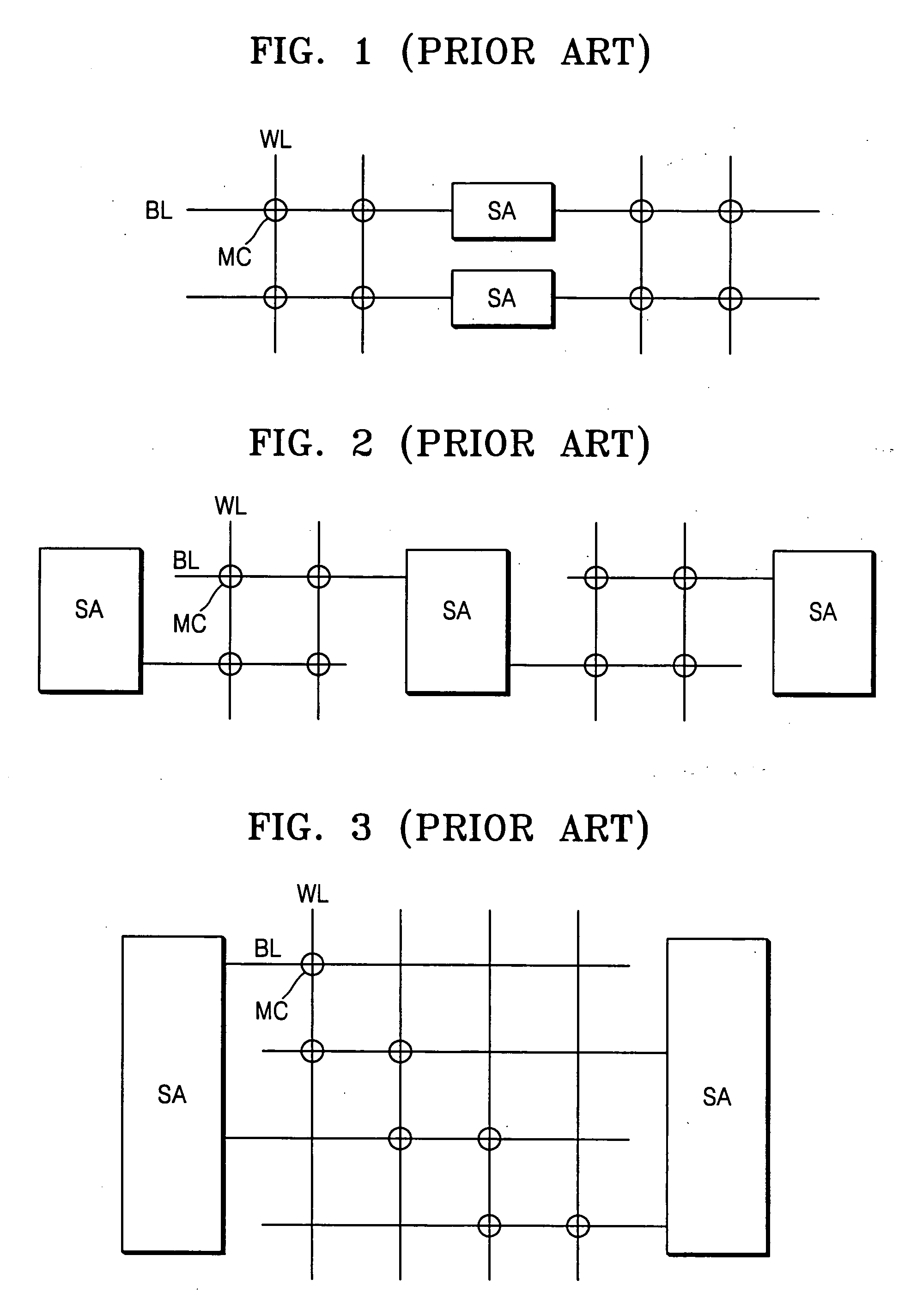
However, since each sense amplifier SA must be designed to be arranged inside the pitch of a bit line BL, the design rules for sense amplifiers SA are tight, reducing flexibility in the design of the layout of the sense amplifiers SA.
Furthermore, since a pair of bit lines BL connected to the sense amplifier SA are not arranged in the same cell array block, one side of the pair of the bit lines BL may be affected by noise generated in one cell array block, while the other side of the pair is not.
Thus, a semiconductor memory device fabricated according to the open bit line method is vulnerable to noise.
However, it is still difficult to design the layout of the sense amplifier SA using the relaxed open bit line method.
In addition, a semiconductor memory device manufactured according to the relaxed open bit line method is vulnerable to noise similar to one manufactured according to the open bit line method.
In addition, since a pair of bit lines BL connected to the sense amplifier SA are installed in the same cell array block, both sides of the pair of the bit lines BL are affected by noise generated in the cell array.
As described above, the area of a memory cell array manufactured according to the open bit line method is reduced, but the memory cell array is vulnerable to noise.

Method used


Image

  • Memory device having shared open bit line sense amplifier architecture
  • Memory device having shared open bit line sense amplifier architecture
  • Memory device having shared open bit line sense amplifier architecture

Examples


Embodiment Construction

[0024] Hereinafter, exemplary embodiments will be described in detail with reference to the accompanying drawings. Like reference numerals denote like elements in the drawings.

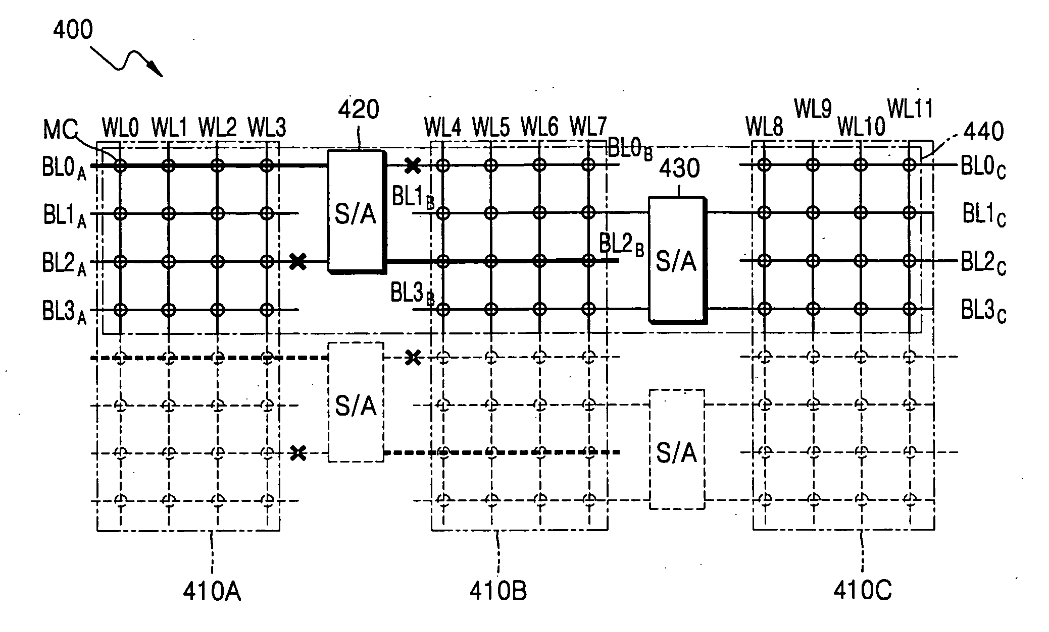
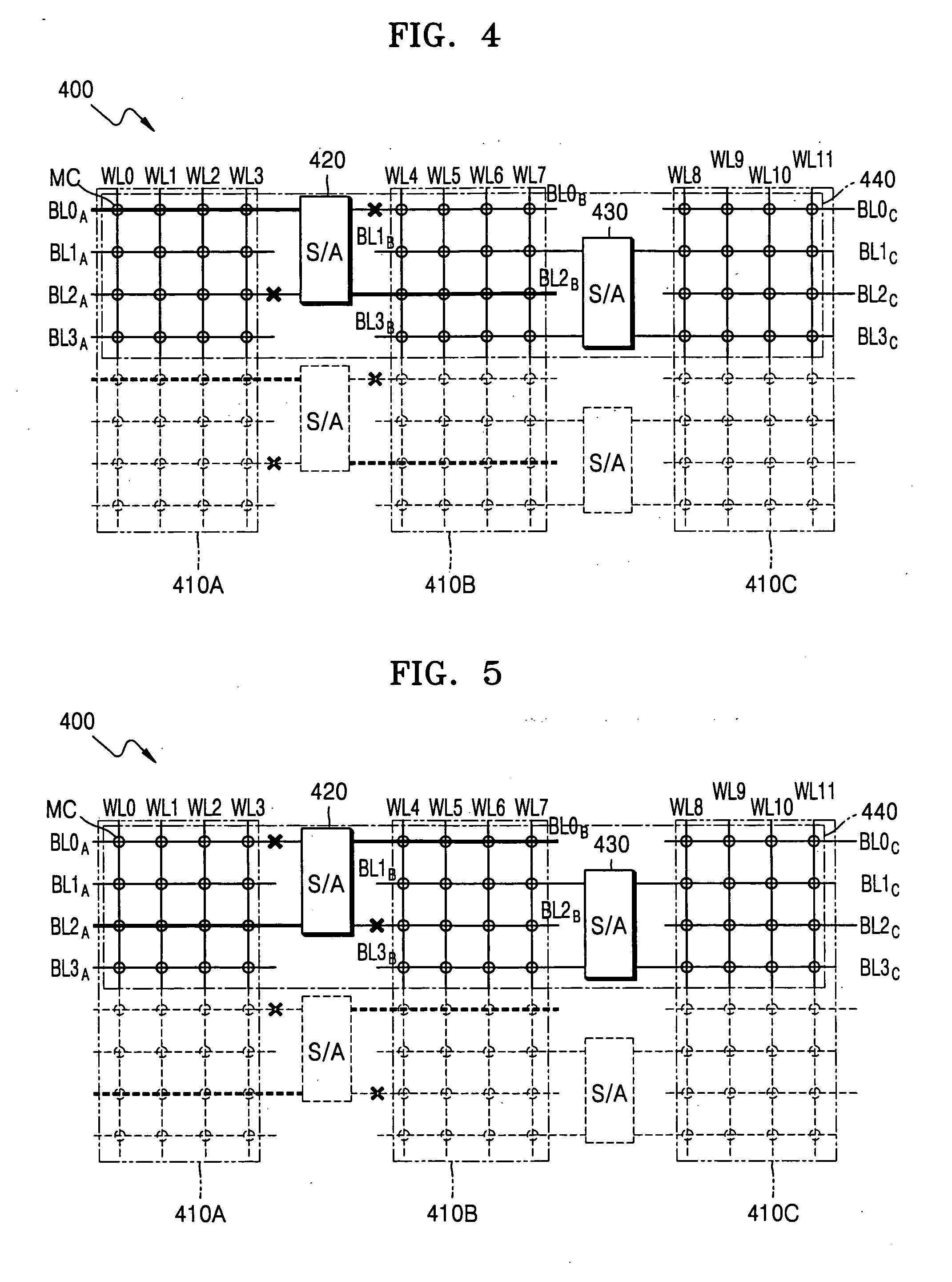
[0025]FIG. 4 illustrates a dynamic random access memory (DRAM) 400 with a shared open bit line sense amplifier architecture according to an embodiment. Referring to FIG. 4, the DRAM 400 includes first through third memory cell arrays 410A, 410B, and 410C, each having cells arranged in the form of a matrix. In the first through third memory cell arrays 410A, 410B, and 410C, DRAM cells MC, each including a transistor and a capacitor, are arranged at intersections of word lines WLi and bit lines BLj (i denotes a number from 0 to 11, and j denotes a number from 0 to 3). That is, the first through third memory cell arrays 410A, 410B, and 410C are manufactured according to the open bit line method. If the minimum design dimension is F, the memory cell MC may have an area of 4F2 or 6F2.

[0026] A first sense amplifie...


PUM


Abstract

Provided is a memory device with a shared open bit line sense amplifier architecture. The memory device includes memory cell arrays, each memory cell array including bit lines, and a sense amplifier configured to couple to at least two bit lines a memory cell array and configured to couple to at least two bit lines of a different memory cell array.

Description

CROSS-REFERENCE TO RELATED PATENT APPLICATIONS [0001] This application claims the priority of Korean Patent Application No. 10-2005-0024076, filed on Mar. 23, 2005, in the Korean Intellectual Property Office, the disclosure of which is incorporated herein in its entirety by reference. BACKGROUND OF THE INVENTION [0002] 1. Field of the Invention [0003] This application relates to semiconductor memory devices, and more particularly, to semiconductor memory devices with a shared open bit line sense amplifier architecture. [0004] 2. Description of the Related Art [0005] In a dynamic random access memory (DRAM), design considerations such as the arrangement of memory cells, each including a transistor and a capacitor, and the arrangement of sense amplifiers that sense and amplify data output from each memory cell are significant in determining the area and the performance of the DRAM. In general, a memory cell array including a sense amplifier is arranged according to an open bit line me...

Claims


Application Information

Patent Timeline
Patent Type & Authority Applications(United States)
IPC IPC(8): G11C7/02
CPCG11C11/4097G11C2207/005A01G33/00A01K61/60Y02P60/60
Inventor YOON, JAE-MANLEE, CHOONG-HOPARK, DONG-GUNLEE, YEONG-TAEKLEE, CHUL
Owner SAMSUNG ELECTRONICS CO LTD
Learn More