
Lens assembly

a technology of lens assembly and lens assembly, which is applied in the direction of photoelectric discharge tubes, instruments, electric discharge lamps, etc., can solve the problems of high cost, high cost of optical lenses, and high cost of lens devices, etc., and achieve the effect of reducing the manufacturing cost of the product with the lens assembly

Inactive Publication Date: 2006-10-05
LUMENS DIGITAL OPTICS
View PDF2 Cites 2 Cited by
  • Summary
  • Abstract
  • Description
  • Claims
  • Application Information

AI Technical Summary

Benefits of technology

"The present invention provides a lens assembly that can be used for various sensors without changing the lens devices. The position of the sensor can be adjusted based on its size or standard. Additionally, the lens assembly includes a spacer that can change the focal length of the sensor for use in various sensors. This helps save manufacturing costs. The lens assembly includes a lens device, a circuit board, a spacer, and a sensor. The spacer is mounted on the circuit board and the sensor is mounted on the spacer. The lens assembly can be used as an objective lens for a visualizer or a CMOS or CCD optical sensor. The lens assembly includes a receptacle portion and a connector for conducting signals and currents. The lens assembly can be used in various applications such as a visualizer or a camera."

Problems solved by technology

Such researches not only involves complex optical, optomechanical and electrical control techniques, but the expense therefor is very high.
Therefore, the price for the optical lens, i.e. the lens device 10, usually is very expensive.
However, the charge for re-designing and producing the particular optical lens is very costly.
Therefore, the manufacturing cost and the price for the products may go up quite substantially and there will be no market for these products.

Method used


Image

  • Lens assembly
  • Lens assembly
  • Lens assembly

Examples


Embodiment Construction

[0032] The present invention will now be described more specifically with reference to the following embodiment. It is to be noted that the following descriptions of preferred embodiment of this invention are presented herein for purposes of illustration and description only; it is not intended to be exhaustive or to be limited to the precise form disclosed.

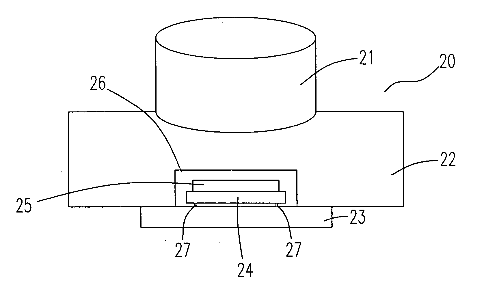
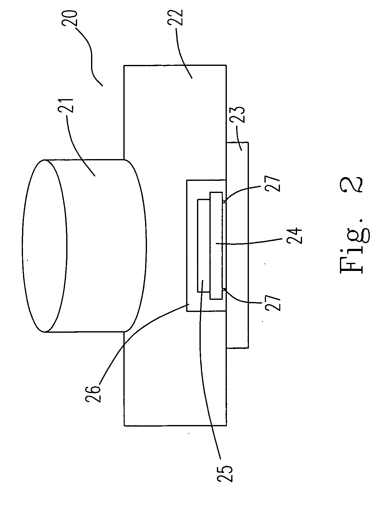
[0033] Please refer to FIG. 2, which is a schematic view showing a lens assembly according to a preferred embodiment of the present invention. The lens assembly includes a lens device 20, a circuit board 23, a spacer 24 and a sensor 25. Further, the lens device 20 includes a lens tube 21 and a lens base 22. The lens base 22 includes a first end and a second end, wherein the lens tube 21 is mounted on the first end and the second end is mounted on the circuit board 23, and the second end further includes a receptacle portion 26. Moreover, the sensor 25 and the spacer 24 are contained within the receptacle portion 26, the sensor 2...


PUM


Abstract

A lens assembly for obtaining an image of an object is provided. The lens assembly includes a lens device receiving a reflected light from the object, a circuit board carrying thereon the lens device, a spacer mounted on the circuit board, and a sensor mounted on the spacer, receiving the reflected light from the lens device and converting the reflected light into a digital signal, thereby generating the image.

Description

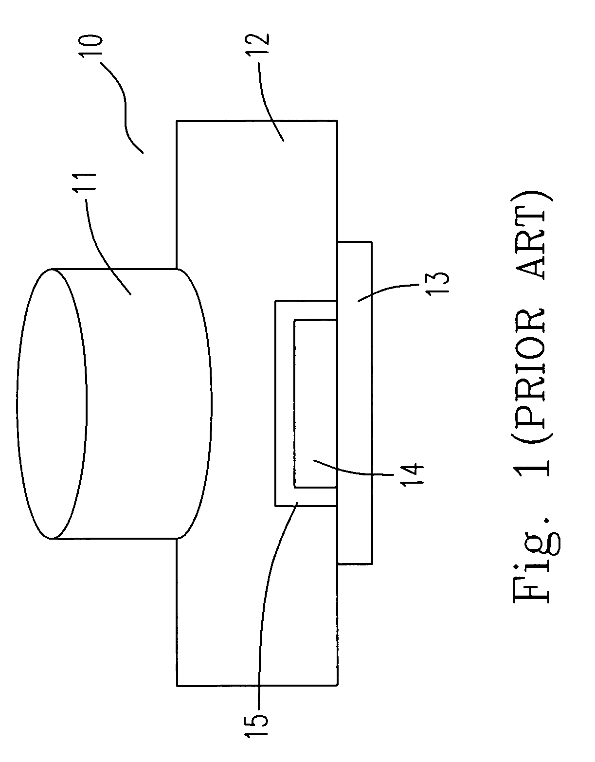
FIELD OF THE INVENTION [0001] The present invention is related to a lens assembly, and more particularly to a lens assembly used for different sizes or standards of sensors without changing any lens devices of the lens assembly. BACKGROUND OF THE INVENTION [0002] Please refer to FIG. 1, which is a schematic view showing a conventional lens structure. The conventional lens structure includes a lens device 10, a circuit board 13 and a sensor 14. Further, the lens device 10 includes a lens tube 11 and a lens base 12, and the sensor 14 is mounted on the circuit board 13. The lens tube 11 further includes an end having a receptacle portion 15 for containing the sensor 13, and the end of the lens tube 11 is mounted on the circuit board 13. Moreover, the circuit board 13 is further used for mounting the lens base 12 thereon. [0003] According to the general imaging theory, a plurality of reflected lights from an object would be received by the lens device 10, and a plurality of focused ligh...

Claims


Application Information

Patent Timeline
Patent Type & Authority Applications(United States)
IPC IPC(8): H01J40/14
CPCH01L27/14625H01L27/14618H01L2924/0002H01L2924/00
Inventor CHEN, CHUN-HSIEN
Owner LUMENS DIGITAL OPTICS
Learn More