Phase-change semiconductor memory device and method of programming the same

a semiconductor memory and phase-change technology, applied in semiconductor devices, digital storage, instruments, etc., can solve the problems of fluctuation in the voltage level of power supply, insufficient write current, and increasing difficulty in generating sufficient pram programming currents from the power supply of such devices

Active Publication Date: 2006-10-05
SAMSUNG ELECTRONICS CO LTD
View PDF10 Cites 47 Cited by
  • Summary
  • Abstract
  • Description
  • Claims
  • Application Information

AI Technical Summary

Problems solved by technology

As the operational voltage level of portable devices continues to decrease, it has become increasingly difficult to generate sufficient PRAM programming currents from the power supplies of such devices.
That is, if the power supply of the PRAM memory device generates low voltage power supply signal (e.g., about 1.8 V), the write current may be insufficient as the result of one or several excessive voltage drops in the write circuit path.
Moreover, another problem can arise when the reset or set operation is performed in a multi-bit cell format, e.g., a×16-bit format.
The accumulative current that is drawn into the memory cells can cause fluctuations in the voltage level of the power supply each time a writing operation is performed.

Method used


Image

  • Phase-change semiconductor memory device and method of programming the same
  • Phase-change semiconductor memory device and method of programming the same
  • Phase-change semiconductor memory device and method of programming the same

Examples


Embodiment Construction

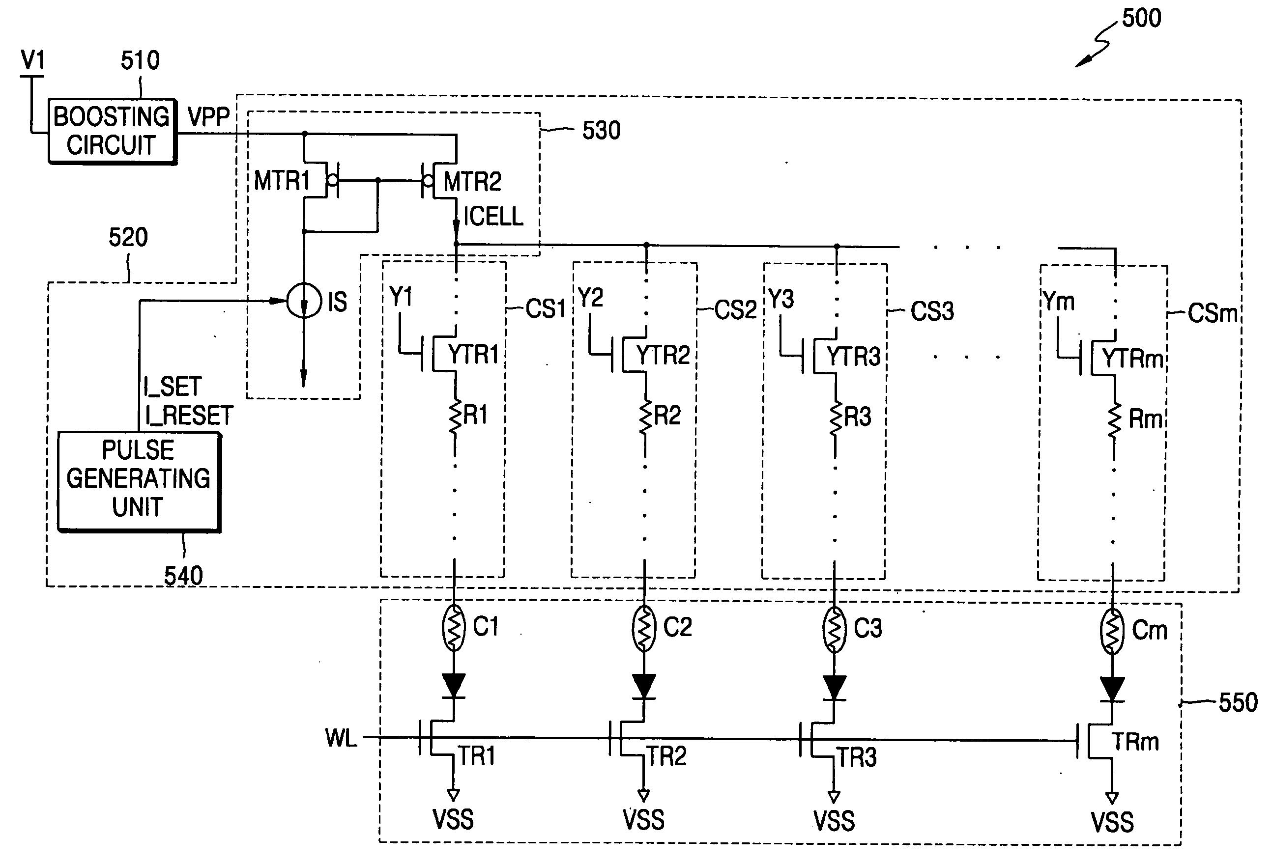
[0029] Hereinafter, exemplary embodiments of the present invention will be described in detail with reference to the accompanying drawings. The drawings are for illustrative purposes only, and are not intended to limit the scope of the invention. FIG. 5 is a circuit diagram of a phase-change semiconductor memory device 500 according to an embodiment of the present invention.

[0030] Referring to FIG. 5, the semiconductor memory device 500 of the illustrated example includes a boosting circuit 510, a write driver 520, and a memory cell array 550.

[0031] The boosting circuit 510 outputs a boosted voltage VPP which is of a higher voltage than an input first voltage V1. The structural configurations of circuits which can function as the boosting circuit 510 are well understood by those skilled in the art, and accordingly, a detailed description thereof is omitted here.

[0032] The memory cell array 550 of this example includes a plurality of phase-change memory cells C1-Cm, diodes D1-Dm, ...


PUM


Abstract

In one aspect, a semiconductor memory device includes a plurality of phase-change memory cells which are programmed according to a write current applied to the phase-change memory cells, a voltage boosting circuit which receives a first voltage and outputs a boosted voltage which is greater than the first voltage, and a write driver which receives the boosted voltage and which generates the write current from the boosted voltage. In another aspect, the write driver generates the write current corresponding to one of a set current pulse and a reset current pulse, and at least one of the set current pulse and the reset current pulse is gradually increased.

Description

BACKGROUND OF THE INVENTION [0001] 1. Field of the Invention [0002] The present invention relates to semiconductor memory devices, and more particularly, the present invention relates phase-change semiconductor memory devices and to methods of programming phase-change semiconductor memory devices. [0003] A claim of priority is made to Korean Patent Application No. 10-2005-0028087, filed on Apr. 4, 2005, in the Korean Intellectual Property Office, the disclosure of which is incorporated herein in its entirety by reference. [0004] 2. Description of the Related Art [0005] A phase-change random access memory (PRAM), also known as an Ovonic Unified Memory (OUM), includes a phase-change material such as a chalcogenide alloy which is responsive to heat so as to be stably transformed between crystalline and amorphous states. Such a PRAM is disclosed, for example, in U.S. Pat. Nos. 6,487,113 and 6,480,438. [0006] The phase-change material of the PRAM exhibits a relatively low resistance in i...

Claims


Application Information

Patent Timeline
Patent Type & Authority Applications(United States)
IPC IPC(8): H01L29/768
CPCG11C13/0004G11C2013/0078G11C13/0069G11C13/0038G11C13/02
Inventor KANG, SANG-BEOMKIM, DU-EUNGOH, HYUNG-ROK
Owner SAMSUNG ELECTRONICS CO LTD
Why Eureka
Try Eureka