Linearized bias circuit with adaptation

Active Publication Date: 2006-10-12
RICHWAVE TECH CORP
View PDF5 Cites 16 Cited by
  • Summary
  • Abstract
  • Description
  • Claims
  • Application Information

AI Technical Summary

Benefits of technology

[0007] Through the temperature compensation characteristics of the linearized bias circuit with adaptation, the DC and AC characteristics of the power amplifier do not shift or deteriorate due to a temperature variation, and when the

Problems solved by technology

When power amplifier is biased with conventional bias circuit, linearity of power amplifier may deteriorate with increased input signal power.
Furthermor

Method used


Image

  • Linearized bias circuit with adaptation
  • Linearized bias circuit with adaptation
  • Linearized bias circuit with adaptation

Examples


first embodiment

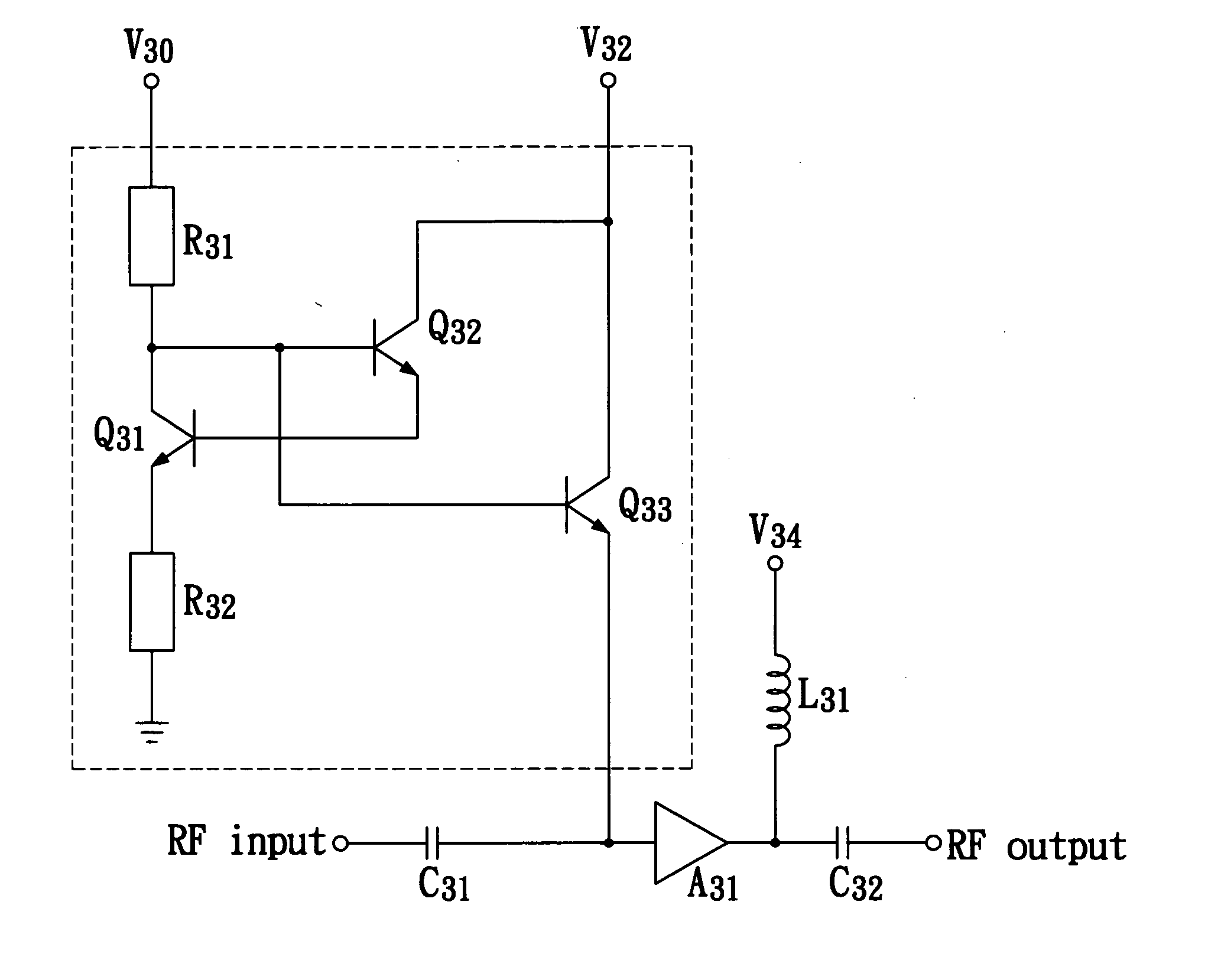
[0014] Reference is made to FIG. 3, which shows a schematic view of a linearized bias circuit with adaptation in a As shown in FIG. 3, a reference voltage source V30, a first voltage source V32, a first resistor R31, a second resistor R32, a first NPN transistor Q31, a second NPN transistor Q32, and a third NPN transistor Q33 are included. First, one end of the first resistor R31 is electrically connected to positive terminal of the reference voltage source V30 and the other end is electrically connected to collector terminal of the first NPN transistor Q31. Additionally, collector terminal of the first NPN transistor Q31 is also electrically connected to base terminals of the second and the third NPN transistors Q32 and Q33, the base terminal thereof is electrically connected to emitter terminal of the second NPN transistor Q32, and the emitter terminal thereof is electrically connected to one end of the second resistor R32. Moreover, collector terminal of the second NPN transisto...

second embodiment

[0015] Reference is made to FIG. 4, which shows a schematic view of a linearized bias circuit with adaptation in a As shown in FIG. 4, a reference voltage source V40, a second voltage source V42, a first resistor R41, a second resistor R42, a first MOS field effect transistor Q41, a second MOS field effect transistor Q42, and a third MOS field effect transistor Q43 are included. Firstly, one end of the first resistor R41 is electrically connected to positive terminal of the reference voltage source V40 and the other end is electrically connected to drain terminal of the first MOS field effect transistor Q41. Additionally, drain terminal of the first MOS field effect transistor Q41 is also electrically connected to gate terminals of the second and the third MOS field effect transistors Q42 and Q43, the gate terminal thereof is electrically connected to source terminal of the second MOS field effect transistor Q42, and the source terminal thereof is electrically connected to one end ...


PUM


Abstract

A linearized bias circuit with adaptation resolves the problem happening to the power amplifier with conventional bias circuit that the DC and AC characteristics of the power amplifier shift or even deteriorate due to a temperature variation. The linearized bias circuit with adaptation has a reference voltage source, a first voltage source, a first resistor, a second resistor, a first NPN transistor, a second NPN transistor, and a third NPN transistor. The present invention has the characteristics of bias current temperature compensation, gain and phase compensations to achieve high linearity for the conventional power amplifier and reducing the DC consumption power. At the same time, the quantity of the required elements and layout area in the present invention are small so that the design complexity can be reduced for improving yield, reducing IC layout area, and reducing cost.

Description

BACKGROUND OF THE INVENTION [0001] 1. Field of the Invention [0002] The present invention is related to a linearized bias circuit with adaptation, and more particularly to an adapted bias circuit design for providing temperature compensation of bias current, linearity improvement, gain, and phase compensation for power amplifier. [0003] 2. Description of Related Art [0004] In all kinds of communication systems, for both transmitter and receiver, linearity is a basic and important specification; for transmitter, power amplifier is an important and indispensable element because it determines the communication distance, communication quality and the battery lifetime. Generally, power amplifier always needs DC bias. When power amplifier is biased with conventional bias circuit, linearity of power amplifier may deteriorate with increased input signal power. Furthermore, the DC and AC characteristics of power amplifier using conventional bias circuit may shift obviously, and even deterior...

Claims


Application Information

Patent Timeline
IPC IPC(8): H03F3/04
CPCH03F1/301H03F1/302H03F2200/391H03F3/189H03F2200/372H03F3/04
Inventor KAO, CHI-HUNGCHEN, CHIH-WEILIN, CHENG-MINCHANG, YUN-SHANWONG, SHYH-CHYI
Owner RICHWAVE TECH CORP
Why Eureka
Try Eureka