Printed circuit board structure
- Summary
- Abstract
- Description
- Claims
- Application Information
AI Technical Summary
Benefits of technology
Problems solved by technology
Method used
Image
Examples
first embodiment
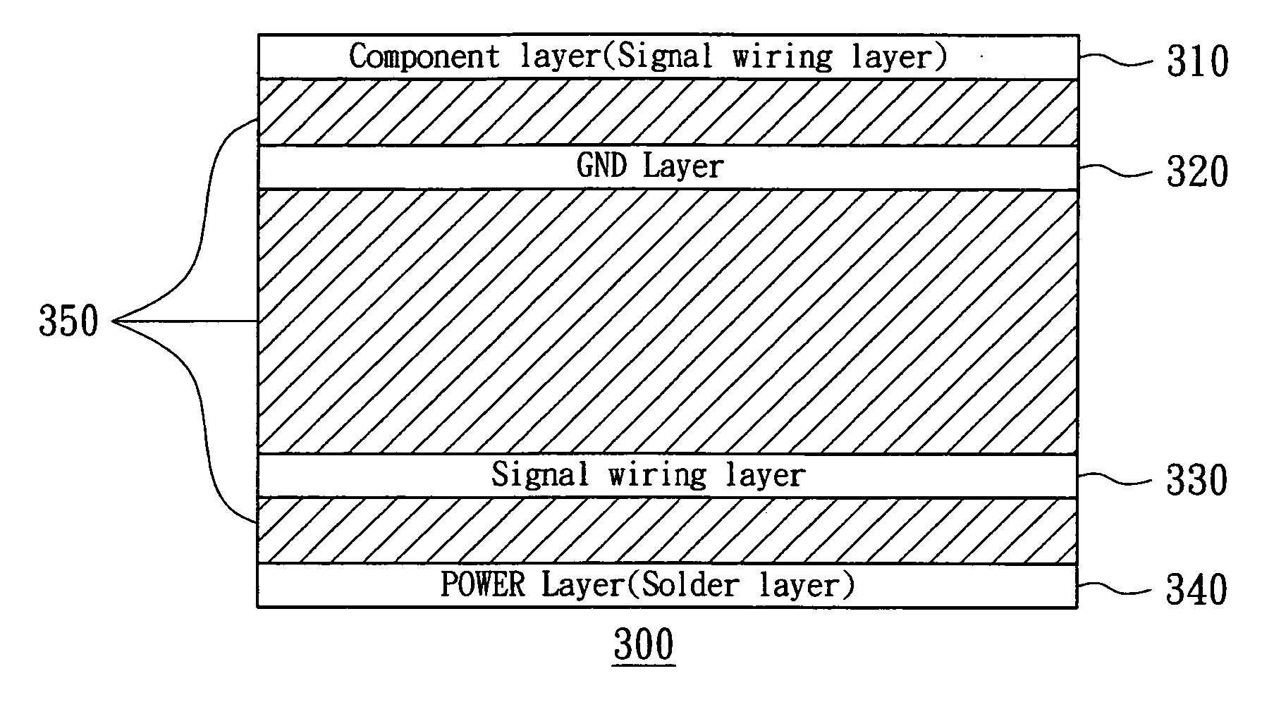
[0021]FIG. 3A shows a front elevation of a printed circuit board structure according to the invention. The printed circuit board 300 provides an example of a four-layer symmetry-type design, which has four conduction layers from top to bottom including a component layer 310, a GND layer 320, a signal wire layer 330 and a POWER layer 340. The conduction layers can be made of any conduction materials, such as copper or gold. Insulation layers 350 are disposed between the conduction layers for insulation, wherein the insulation layers are made of insulation materials having a specific dielectric coefficient, such as glass fibers. The component layer 310, a kind of signal wire layer, is exposed at the surface of the printed circuit board 300, for configuring wires coupled to the operation devices (not shown in the figure) on the printed circuit board 300. The GND layer 320 is used as a signal reference layer for the component layer 310 and disposed close to the component layer 310 in th...
second embodiment
[0025] Referring to FIG. 4A, a front elevation of a printed circuit board structure according to the invention is shown. The printed circuit board 400, a symmetry-type design, has six conduction layers including a component layer 410, a GND layer 420, a POWER layer 430, a signal wire layer 440, a GND layer 450, and a POWER layer 460 in order from top to bottom. The conduction layers can be made of any conduction material, such as copper or gold. Insulation layers 405 are disposed between the conduction layers for insulation, wherein the insulation layers 405 are made of an insulation material having a specific dielectric coefficient, such as glass fibers. The component layer 410 is a kind of signal wire layer exposed at the upper surface of the printed circuit board 400 for configuring wires coupled to the operation devices (not shown in the figure) on the printed circuit board 400. The GND layer 420 is used as a signal reference layer for the component layer 410 and disposed close ...
PUM
 Abstract
Description
Claims
Application Information


